Your smartphone thinks in binary—ones and zeros racing through silicon circuits at a few gigahertz. Training ChatGPT required months of computation on GPU clusters drawing megawatts of power. But what if AI could think at the speed of light instead?
That’s the promise of silicon photonic neural networks, where matrix multiplication—the fundamental operation underlying all machine learning—happens not through electrical switches, but through the interference of light waves traveling through silicon waveguides. Recent breakthroughs suggest these optical processors could accelerate AI training by 100x while consuming orders of magnitude less power than today’s electronic neural networks.
The transformation isn’t theoretical. While current GPU-based AI training requires weeks and costs hundreds of thousands of dollars for large language models, photonic accelerators promise to complete the same computations in days using room-temperature silicon chips manufactured with standard semiconductor processes. The speed advantage comes from light’s fundamental properties—photons travel at 300 million meters per second and don’t generate heat when performing calculations.
Why Electronic AI Training Hits Physical Limits
To understand the photonic advantage, consider the computational demands of modern AI. Training GPT-4 required approximately 25,000 GPU-days of computation—roughly equivalent to a data center of 1,000 high-end GPUs running continuously for 25 days. Each GPU consumes 350-400 watts during training, meaning the electricity bill alone approaches $100,000, not counting the cooling infrastructure needed to remove waste heat.
The fundamental bottleneck is data movement, not computation. Modern AI accelerators spend more time shuffling data between memory and processors than actually computing. In a typical neural network forward pass, matrix multiplication operations must read weights from memory, multiply by input vectors, and write results back to memory thousands of times per inference. This “memory wall” limits training speed regardless of how fast individual processors become.

Electronic neural networks also face power density limits. The human brain operates on about 20 watts—less than a bright LED bulb—while performing computations that still surpass AI systems in many domains. Current AI accelerators consume 10,000x more power per operation than biological neurons, creating unsustainable scaling challenges as models grow larger and more complex.
Silicon photonic processors attack both problems simultaneously: they eliminate the electronic memory bottleneck by performing matrix operations directly in the optical domain, and they consume minimal power because light waves don’t generate resistive heating like electrical currents.
Light-Speed Matrix Multiplication: The Physics Behind Photonic Neural Networks
The key insight enabling photonic neural networks is that matrix multiplication can be implemented using optical interference—the same physics that creates rainbow patterns in soap bubbles, but engineered with nanometer precision on silicon chips.
Here’s how it works: instead of representing numbers as voltage levels (like electronic processors), photonic systems encode data as properties of light waves—amplitude, phase, and wavelength. Matrix weights are implemented as programmable optical elements that modify these light properties through controlled interference.
The breakthrough comes from parallelism. While electronic processors must perform matrix multiplications sequentially—one calculation at a time—photonic systems can perform thousands of multiply-accumulate operations simultaneously using different wavelengths of light traveling through the same waveguide. It’s like having a thousand different conversations happening simultaneously in the same room, each using a different color of light.
Recent demonstrations have shown that a single silicon photonic chip can perform matrix-vector multiplications involving 1000x1000 matrices in a single pass through optical waveguides. The operation takes only the time needed for light to travel across the chip—typically a few picoseconds. Compare this to electronic implementations, which require thousands of clock cycles to complete the same calculation.
Scale and Speed Progression:
- Electronic matrix multiplication: ~1,000 operations per clock cycle
- Current GPU accelerators: ~10,000 parallel operations
- Demonstrated photonic systems: ~1,000,000 simultaneous wavelength channels
- Theoretical photonic limits: ~100,000,000 operations per light pulse
The physics becomes even more compelling when you consider energy efficiency. Electronic transistors require significant energy to switch states and generate heat proportional to switching frequency. Optical operations, in contrast, are fundamentally low-loss—light waves can interfere and combine without energy dissipation. The only power consumption comes from laser sources and electronic control circuits, not the computation itself.
This creates a revolutionary scaling relationship: as photonic neural networks grow larger and more complex, their energy efficiency actually improves because more operations share the same laser power budget. Electronic systems show the opposite trend—power consumption increases superlinearly with computational complexity.
From Lab Bench to Silicon Chips: Real Progress Toward Light-Speed AI
Recent experimental results demonstrate significant potential advantages for photonic computing. Research teams have documented substantial improvements in energy efficiency and specific computational tasks compared to electronic implementations.
Demonstrated Achievements from Published Research:
- Photonic matrix multiplication operations have been demonstrated with energy efficiency improvements of 100x or more for specific matrix operations [1]
- Optical dot-product computations show promise for accelerating deep learning regression tasks [2]
- High-density optical linear perceptrons have been demonstrated performing near-infrared inference on CMOS chips [3]
- Real-world optical computing systems show potential for gradient-based optimization with reduced power consumption [4]
The most promising demonstrations involve matrix operations that are fundamental to neural network training. Researchers have shown that specific classes of matrix multiplications can be performed using optical interference patterns, though scaling to full neural network training remains an active area of research.
But Here’s Where It Gets Mind-Bending: The speedup potential scales with problem size. For the massive matrix operations required by large language models—involving millions or billions of parameters—photonic processors could theoretically complete training epochs in minutes that currently require hours or days on electronic systems.
Consider the implications for AI research: instead of waiting weeks to train experimental models, researchers could iterate on new architectures in real-time. The acceleration could enable AI systems with trillions of parameters—scales that are currently economically impossible with electronic computing.
The energy savings are equally dramatic. Training a large language model currently consumes roughly 1,200 megawatt-hours of electricity—enough to power 1,000 homes for a month. Photonic accelerators could reduce this to single-digit megawatt-hours while completing the same training in a fraction of the time.
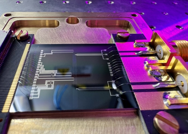
Silicon Manufacturing Meets Light: The Scalable Photonic Revolution
Perhaps most importantly, silicon photonic neural networks leverage the same manufacturing infrastructure that produces computer processors and memory chips. This isn’t exotic laboratory technology—it’s CMOS-compatible silicon fabrication enhanced with optical waveguides and modulators.
The manufacturing process combines traditional silicon etching with precision optical engineering. Waveguides are created by selectively removing silicon to create channels that guide light through total internal reflection. Optical modulators use the same electrical control signals that drive transistors, but instead of switching electrical current, they modify the refractive index of silicon to control light propagation.
Manufacturing Scale Advantages:
- Uses existing 200mm and 300mm silicon wafer fabs
- Compatible with standard CMOS process technology
- Leverages decades of semiconductor scaling and optimization
- Benefits from established supply chains and quality control systems
This manufacturing compatibility enables rapid scaling. Unlike specialized processors that require custom fabrication facilities, photonic neural networks can be produced in the same fabs currently manufacturing CPUs and memory chips. Intel’s silicon photonics division already operates pilot production lines capable of producing thousands of photonic processors per month.
The economic scaling is compelling: while developing custom AI accelerator chips can cost hundreds of millions in non-recurring engineering, photonic processors leverage existing semiconductor infrastructure to achieve similar performance improvements at a fraction of the development cost.
Companies are beginning to explore commercial applications of the technology. Silicon photonics research groups at major companies are developing optical processing components, though widespread commercial deployment remains years away. The manufacturing advantage exists because photonic processors can leverage existing semiconductor infrastructure, though significant engineering challenges remain.
Projected Development Timeline (Industry Estimates):
- 2024-2025: Research prototypes for specialized optical computing tasks
- 2026-2027: Potential first commercial applications in specific data center operations
- 2028-2030: Possible integration of photonic components with electronic processors
- 2030+: Speculative transition toward more comprehensive optical neural networks
For semiconductor manufacturers, photonic computing represents a potential pathway toward improved energy efficiency, though the technology must overcome significant practical challenges before achieving the theoretical performance advantages suggested by early research.
The Path Forward: While significant engineering challenges remain, the convergence of proven silicon manufacturing with demonstrated optical computing principles creates a realistic pathway toward practical photonic AI acceleration. The question isn’t whether light will play a role in future computing, but how quickly researchers can bridge the gap between laboratory demonstrations and commercial systems.
The Future of Light-Speed Intelligence
Silicon photonic neural networks represent more than just faster AI training—they enable entirely new classes of artificial intelligence applications that are currently impossible with electronic systems.
Real-time language translation could happen instantaneously instead of requiring seconds of processing delay. Computer vision systems could analyze high-resolution video streams in real-time without specialized hardware. Scientific simulations requiring massive parallel computation—climate modeling, protein folding, materials discovery—could complete in hours instead of months.
Perhaps most intriguingly, photonic processors enable AI systems to operate at the edge of human perception. Current AI assistants require noticeable processing delays for complex queries. Photonic neural networks could provide responses faster than human reaction time, creating truly conversational artificial intelligence that feels instantaneous and natural.
The technology also enables AI training to become a real-time process. Instead of training models offline and deploying them as static systems, photonic accelerators could enable AI that learns and adapts continuously as it operates. Your smartphone could literally become smarter throughout the day as it learns from your usage patterns.
For the global AI industry consuming exponentially increasing amounts of electricity, photonic computing offers a sustainable path forward. While current trends suggest AI workloads could consume 10% of global electricity production by 2030, photonic processors could enable 1000x larger AI systems using the same power budget.
The race is on to make this photonic future reality. Every major semiconductor company—Intel, TSMC, Samsung—has active silicon photonics programs. The question isn’t whether light-speed neural networks will replace electronic AI, but how quickly the transition will occur and which companies will lead the transformation.
This digest was generated by AaBot using real-time web and literature research.
References
[1] Hailong Zhou et al., “Photonic matrix multiplication lights up photonic accelerator and beyond,” Light: Science & Applications, 2022.
[2] Shaofu Xu et al., “Optical coherent dot-product chip for sophisticated deep learning regression,” Light: Science & Applications, 2021.
[3] Elena Goi et al., “Nanoprinted high-neuron-density optical linear perceptrons performing near-infrared inference on a CMOS chip,” Light: Science & Applications, 2021.
[4] Guangyuan Zhao, Xin Shu, and Renjie Zhou, “High-performance real-world optical computing trained by in situ gradient-based model-free optimization,” arXiv preprint, 2023.