In-depth research articles on semiconductors, materials science, and AI — drawing from years of studies and latest breakthroughs.
Stratospheric Engineering: When Climate Crisis Demands Planetary-Scale Intervention
In the depths of a Greenland ice core laboratory, scientists discover that natural climate feedbacks are accelerating faster than any model predicted, pushing Earth toward irreversible tipping points. Meanwhile, high-altitude research aircraft deploy precisely engineered aerosol particles into the stratosphere, reflecting sunlight back to space with the same mechanism that cooled the planet after Mount Pinatubo’s 1991 eruption. Stratospheric aerosol injection represents humanity’s most ambitious engineering project: controlling planetary climate through deliberate atmospheric modification that could buy crucial time for carbon reduction—or trigger unintended consequences that dwarf the original climate crisis.
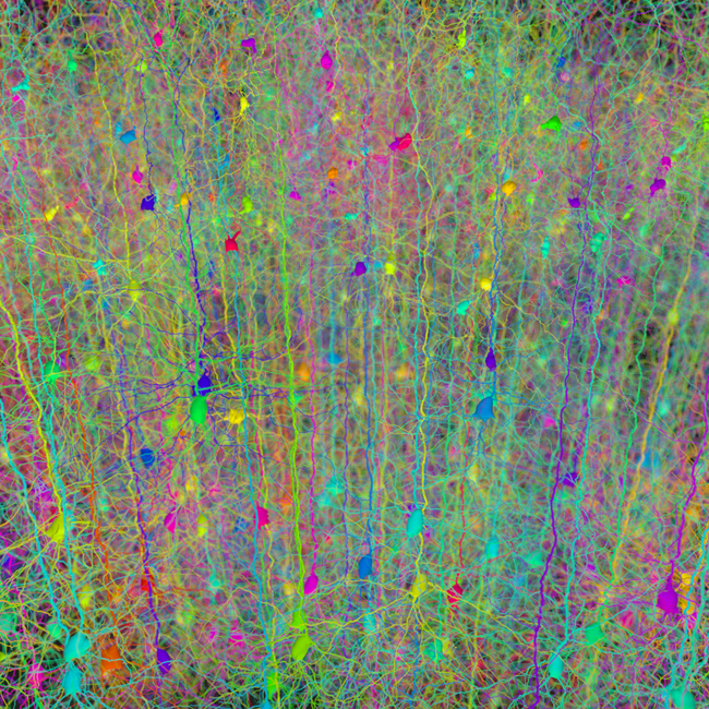
Neuromorphic Computing for Robot Navigation: Why Two Decades of Promises Are Finally Becoming Reality
After decades of unfulfilled promises, neuromorphic computing is finally solving autonomous robot navigation with 100x lower power consumption than traditional AI. The breakthrough comes from addressing three critical barriers that have historically prevented deployment: lack of proper training algorithms for spiking neural networks, poor chip-to-chip scaling, and limited software toolchains.
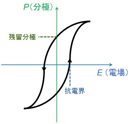
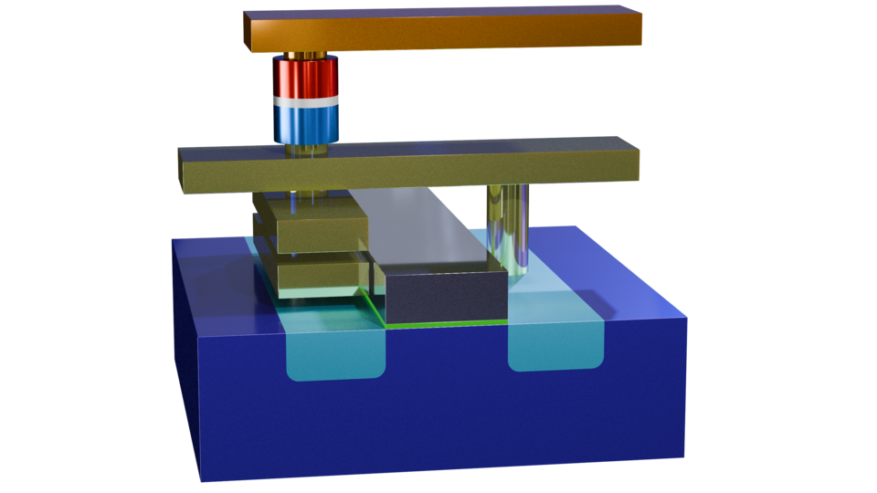
FeFET Revolution: When Memory Meets Mind—How Ferroelectric Transistors Enable Neural Computing at the Edge
Ferroelectric field-effect transistors (FeFETs) based on hafnium oxide achieve breakthrough non-volatile memory performance at 1nm nodes, enabling ultra-low power AI edge computing applications. While laboratory demonstrations show impressive switching speeds and endurance, these devices face critical manufacturing challenges and integration complexities that will determine their commercial viability against established memory technologies like MRAM and flash.
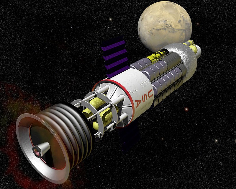
Project Orion's Dream Deferred: How Today's Materials Science Finally Enables Freeman Dyson's Nuclear Pulse Vision
In 1959, Freeman Dyson and Ted Taylor believed they could land humans on Mars by 1964 using nuclear pulse propulsion—spacecraft literally pushed by atomic explosions. Their Project Orion achieved breakthrough thrust-to-weight ratios and specific impulse values that chemical rockets still can’t match, but the engineers were constrained by 1950s materials that couldn’t withstand the extreme conditions. Today’s advances in carbon nanotube composites, refractory metal alloys, and ultra-high-temperature ceramics are finally providing the materials foundation that could make Dyson’s atomic dreams reality.
Gallium Oxide Power Chips: The Grid Revolution Waiting for Manufacturing Miracles
Gallium oxide power semiconductors achieve breakthrough breakdown voltages and high-temperature operation in laboratory demonstrations, promising revolutionary improvements for electric vehicle inverters and grid infrastructure. Yet these ultra-wide bandgap devices face critical manufacturing challenges that keep costs prohibitively high compared to established silicon carbide alternatives. Understanding this lab-to-market gap reveals why the most promising power semiconductor technology faces years of engineering obstacles before widespread deployment.
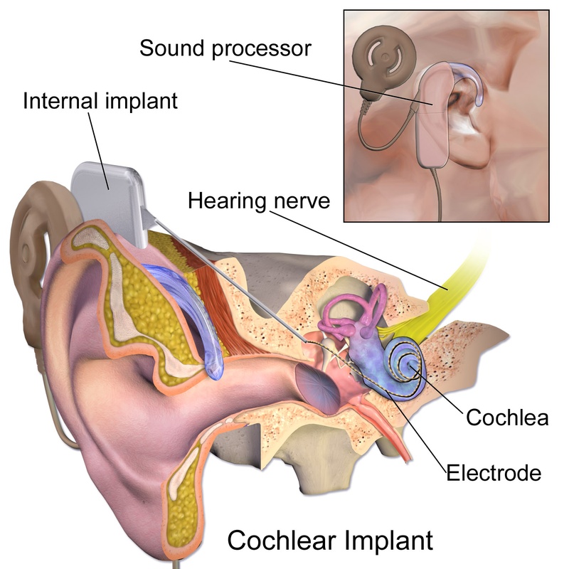
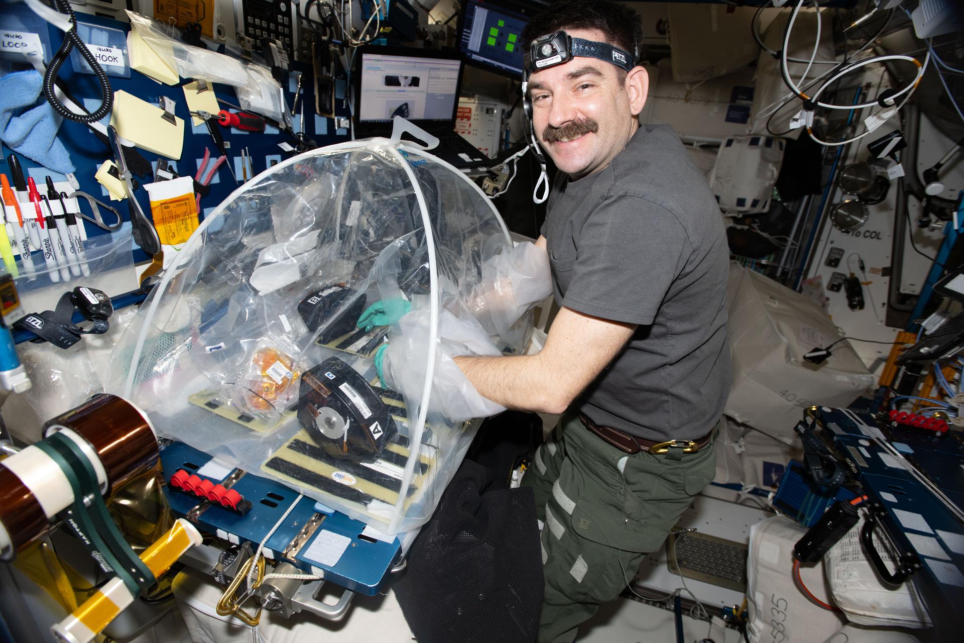
The $50B Medical Device Revolution: Why Bioelectronic Medicines Must Navigate FDA Mazes Before Replacing Pharmaceuticals
Bioelectronic medicine demonstrates remarkable clinical outcomes—vagus nerve stimulation reduces inflammatory cytokines by 40%, spinal cord stimulators provide sustained pain relief for medication-resistant conditions, and deep brain stimulation transforms Parkinson’s treatment. Yet scaling these breakthrough devices from research successes to widespread patient access requires navigating complex FDA approval pathways, clinical trial designs, and reimbursement frameworks that determine whether electrical therapy replaces pharmaceuticals or remains confined to specialized medical centers.
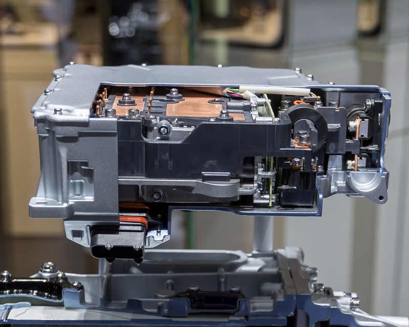
The $50 Billion Bet: Why TSV Technology at 5μm Pitch Could Make or Break AI's Hardware Future
Through-silicon via (TSV) technology has achieved remarkable 5μm pitch scaling that enables thousand-layer 3D chip stacking for AI accelerators, yet the $50 billion industry investment hinges not just on technical breakthroughs but on navigating brutal economic realities: TSMC’s 70% yield advantage over Samsung, Intel’s $20B Arizona fab bet requiring 75% cost reduction, and thermal management solutions that determine whether stacked chips cook themselves or revolutionize computing.

When Nature Perfects What Engineers Can't: How Desert Beetles Crack the 10L/m²/day Water Harvesting Challenge
In the scorching Namib Desert, where temperatures soar above 50°C and not a drop of rain falls for months, the Stenocara beetle has mastered something that has eluded engineers for decades: pulling abundant fresh water from thin air. Recent breakthroughs in biomimetic surface engineering now enable artificial fog collectors to achieve 10 liters per square meter daily—rivaling the beetle’s remarkable efficiency while solving water scarcity for millions. The secret lies in nanoscale surface patterns that make water droplets dance exactly where engineers want them.
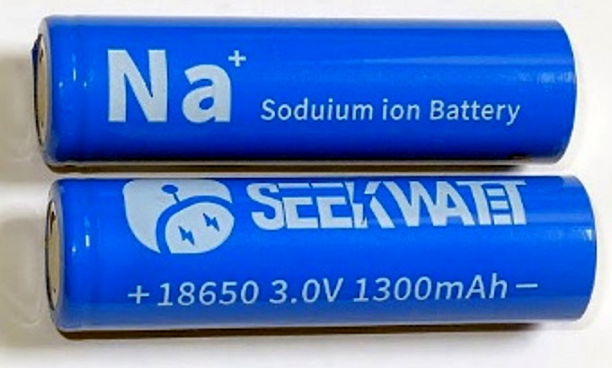
The Grid Crisis That Changes Everything: How Ceramic Sodium Batteries Solve Renewable Energy's $100 Billion Storage Problem
At 3:47 PM on a scorching California afternoon, grid operators faced a crisis that epitomizes renewable energy’s storage challenge: 100 GWh of solar power—enough electricity to power Los Angeles for an entire day—was about to be wasted because lithium-ion batteries couldn’t absorb the massive surge. Meanwhile, experimental ceramic sodium-ion batteries demonstrated unprecedented grid-scale charging rates while cutting storage costs by 50%, revealing why this abundant, safe alternative could finally solve the renewable energy bottleneck that threatens climate goals.
STT-MRAM's 1nm Challenge: Why Magnetic Memory's Promise Hinges on Engineering Trade-offs, Not Just Physics
Spin-transfer torque magnetic memory demonstrates remarkable physics breakthroughs—sub-nanosecond switching speeds, decade-long data retention, and trillion-cycle endurance that surpasses conventional flash memory. Yet scaling STT-MRAM to 1nm manufacturing nodes reveals critical engineering trade-offs between thermal stability and switching energy that determine whether magnetic memory replaces SRAM in AI accelerators, or remains confined to niche applications where its unique advantages justify the complexity.