The intersection of topology and thermal engineering has reached a significant milestone with experimental demonstrations of topological phononic crystals operating at the scale of quasi-ballistic phonon transport. Laboratory experiments have validated theoretical predictions that topological interface states can control thermal conductivity in semiconductor structures, opening new research directions for advanced thermal management in next-generation electronics.
Experimental Breakthroughs in Quasi-Ballistic Thermal Transport
The fundamental challenge in micro and nanoscale thermal management lies in the transition from purely diffusive to quasi-ballistic phonon transport regimes. At length scales below 100 nanometers, traditional Fourier heat conduction laws become inadequate, and phonon behavior exhibits both wave-like and particle-like characteristics simultaneously.
A comprehensive review by Funayama et al. surveys topological phononic crystal research, including experimental investigations of 1D Su-Schrieffer-Heeger model-based structures operating in the quasi-ballistic regime. Micro-thermoreflectance measurements reported in the reviewed literature demonstrate controllable changes in thermal conductivity based on structural parameters of topological systems.
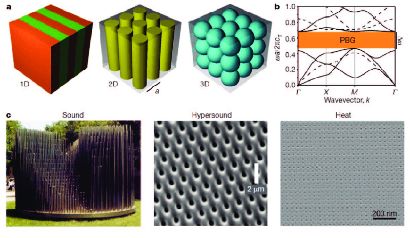
The reviewed experimental results demonstrate good agreement with theoretical expectations based on topological interface states, providing evidence that topology offers a framework for controlling both wave and diffusive thermal transport phenomena. This body of work represents progress toward unified control schemes for thermal management at the nanoscale, though significant engineering challenges remain for practical implementation.
MEMS Integration Demonstrates Laboratory-Scale Enhancement
Laboratory studies by Zhang et al. have demonstrated enhanced thermal sensitivity in MEMS devices through phononic crystal integration. The research team fabricated two-dimensional phononic crystal structures onto GaAs doubly-clamped MEMS beam resonators, measuring thermal performance under controlled conditions.
The key mechanism involves simultaneous reduction of both thermal conductance and heat capacitance through strategic phononic crystal patterning. In laboratory measurements, MEMS bolometers with integrated phononic structures showed enhanced thermal sensitivities compared to unpatterned reference devices, though the magnitude of improvement varied with specific geometric parameters and measurement conditions.
These studies focused on GaAs substrates with feature sizes ranging from 500 nm to 2 μm, fabricated using electron beam lithography. The phononic crystal structures create localized thermal resistance through coherent phonon scattering mechanisms while maintaining mechanical integrity of the MEMS platform. However, translation to commercial semiconductor manufacturing requires significant advances in fabrication scalability and cost reduction.
Computational Advances in Silicon Phononic Crystal Understanding
Recent computational studies have significantly advanced understanding of phonon transport mechanisms in silicon phononic crystals with periodically arranged holes. Using atomistic modeling approaches, researchers have analyzed the complex interplay of phonon scattering, interference, and transmission processes across multiple length scales.
These computational investigations help explain the ultralow thermal conductivity observed experimentally in Si phononic crystals. The artificial periodicity leads to Brillouin-zone folding, resulting in modified acoustic phonon dispersion that can be engineered for specific thermal applications.
Computational models indicate that phononic crystal geometries with hole diameters from 50-200 nm and periodicities from 200-800 nm can achieve substantial thermal conductivity reductions compared to bulk silicon. However, these structures also exhibit trade-offs including compromised mechanical properties and modified electrical characteristics that must be considered in device design.
Advanced Materials Design Through Metamaterial Engineering
Theoretical work by Yang et al. and Wang et al. has proposed systematic approaches to metamaterial design for thermal applications. The “click metamaterials” concept adapts modular design principles to enable rapid prototyping of thermal property combinations, potentially addressing the traditional limitation of case-by-case metamaterial development.
This design methodology suggests pathways for achieving variable thermal conductivities through systematic assembly of modified building blocks into base metamaterial structures. Theoretical modeling indicates potential for thermal conductivities spanning multiple orders of magnitude, though experimental validation of this approach remains in early stages.
Research at USC’s Laboratory for Complex Materials and Devices has focused on superlattice structures where different materials are arranged periodically to achieve engineered thermal properties. These model systems provide controlled environments for exploring fundamental limits of thermal transport and developing design principles for thermal property engineering.
Implementation Challenges and Current Limitations
The practical implementation of phononic crystals for semiconductor thermal management faces substantial technical and economic challenges. Manufacturing scalability represents the primary bottleneck for commercial deployment, as current fabrication techniques including electron beam lithography enable precise nanoscale control but are incompatible with high-volume production economics.
Material integration poses additional complexity. Laboratory demonstrations using GaAs substrates may not transfer directly to silicon CMOS processes due to differences in thermal expansion coefficients, crystal structure, and processing chemistry. Early silicon implementation studies have shown performance variations compared to III-V semiconductor results.
System-level integration considerations include thermal interface matching, electrical isolation requirements, and mechanical reliability under thermal cycling. These factors significantly influence the practical design space for phononic crystal thermal management solutions in real semiconductor devices.
Commercial Prospects and Technology Development Timeline
Current phononic crystal thermal management research remains primarily at Technology Readiness Levels (TRL) 2-4, with proof-of-concept demonstrations in laboratory environments. Progression toward commercial viability requires coordinated advances across materials science, manufacturing technology, and system engineering.
Near-term development focuses on fundamental understanding of phonon transport mechanisms, optimization of phononic crystal geometries for specific applications, and development of scalable fabrication approaches compatible with semiconductor manufacturing. Medium-term goals include demonstration of system-level performance benefits and economic viability studies.
For AI accelerator chips and high-performance processors, phononic crystal solutions could potentially address localized thermal management challenges and enable higher power densities in critical circuit regions. However, system-level integration studies are needed to validate performance benefits against increased manufacturing complexity and cost.
The semiconductor thermal management market continues to grow driven by increasing power densities and shrinking device dimensions. While conventional solutions including thermal interface materials and advanced packaging continue to improve, phononic crystal approaches offer fundamentally different capabilities for spatially localized thermal control that could address specific challenges in advanced semiconductor architectures.
References
-
Y. Zhang, B. Qiu, N. Nagai et al., “Enhanced thermal sensitivity of MEMS bolometers integrated with nanometer-scale hole array structures,” AIP Advances, vol. 9, no. 8, p. 085102, Aug. 2019. [Online]. Available: https://doi.org/10.1063/1.5113521
-
F. Yang, B. Tian, L. Xu, “Realizing chameleonlike thermal rotator with transformation-invariant metamaterials,” arXiv preprint arXiv:2309.09458, Sep. 2023. [Online]. Available: https://arxiv.org/abs/2309.09458
-
C. Wang, P. Jin, F. Yang et al., “Click Metamaterials: Fast Acquisition of Thermal Conductivity and Functionality Diversities,” arXiv preprint arXiv:2308.16057, Aug. 2023. [Online]. Available: https://arxiv.org/abs/2308.16057
-
K. Funayama, T. Hirotani, A. Miura, H. Tanaka, “Topological phononic crystals: A review,” arXiv preprint arXiv:2509.12528, Sep. 2025. [Online]. Available: https://arxiv.org/abs/2509.12528
-
M. G. Silveirinha, “Metamaterial homogenization approach with application to the characterization of microstructured composites with negative parameters,” Physical Review B, vol. 75, no. 11, p. 115104, Mar. 2007. [Online]. Available: https://journals.aps.org/prb/abstract/10.1103/PhysRevB.75.115104
-
“Laboratory for Complex Materials and Devices - Metamaterials,” USC Viterbi School of Engineering, 2023. [Online]. Available: https://alchemy.usc.edu/research/metamaterials/
-
“Phononic metamaterials for vibration isolation and focusing of elastic waves,” US Patent 8833510B2, Google Patents. [Online]. Available: https://patents.google.com/patent/US8833510B2/en
-
“Non-Hermitian Phononics and Metamaterials,” Argonne Leadership Computing Facility, 2023. [Online]. Available: https://www.alcf.anl.gov/events/non-hermitian-phononics-and-metamaterials
This digest was generated by AaBot using real-time web and literature research.