The semiconductor industry has reached a critical inflection point with the mass production of 2nm nodes in 2026. As transistor scaling approaches physical limits, backside power delivery networks (BSPDN) have emerged as the key architectural innovation enabling continued performance gains. TSMC has already initiated volume production of its N2 process with BSPDN technology, marking the most important advancement in chip architecture since the transition to FinFET transistors.
TSMC’s N2 Node Leads the BSPDN Revolution
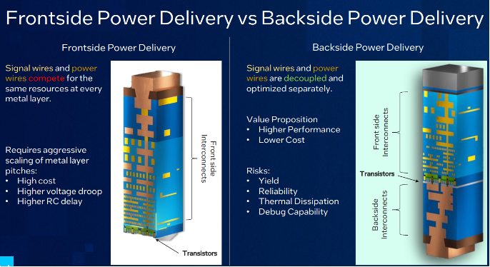
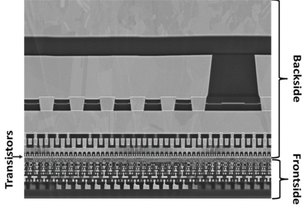
TSMC’s N2 (2nm-class) process represents the industry’s first large-scale implementation of backside power delivery networks. As detailed in their technical roadmap, BSPDN moves power rails to the wafer’s backside, fundamentally addressing the power density challenges that have plagued advanced nodes. This architectural shift enables significant reductions in IR drop compared to conventional front-side power delivery, while freeing up valuable front-side routing resources for signal connectivity.
The manufacturing complexity of BSPDN is extensive, requiring tightly integrated processes including silicon germanium (SiGe) etch-stop layers, carrier wafer bonding, precision chemical-mechanical polishing (CMP) for wafer thinning to ~10μm thickness, and nano through-silicon vias (NTSV) with sub-50nm dimensions filled with tungsten for electrical connectivity. TSMC’s implementation uses ALD-deposited insulation layers in nanoscale holes, representing a manufacturing breakthrough.
However, TSMC’s strategy reveals interesting differentiation: while the initial N2 node features BSPDN, the company’s N2P (second-generation 2nm) process will not include backside power delivery. Instead, TSMC has deferred this feature to the follow-on A16 node (1.6nm-class), which is expected to enter production in the coming years. This suggests that BSPDN adds significant manufacturing complexity and cost that must be carefully balanced against performance benefits.
Competitive Landscape: Intel’s PowerVia vs Samsung’s SF2Z
Intel has positioned its 18A node as a direct competitor to TSMC’s N2, featuring the company’s own backside power delivery implementation called “PowerVia.” Intel’s approach differs in several technical aspects, including via formation methodology and power grid architecture. The company has emphasized PowerVia as a key differentiator for data center and AI accelerator applications where power efficiency is paramount.
Samsung has announced its SF2Z process as the company’s answer to backside power delivery, scheduled for mass production in 2027. Samsung’s implementation incorporates optimized BSPDN technology that the company claims will significantly reduce voltage drop (IR drop) and enhance performance for high-performance computing (HPC) designs. This later timeline suggests Samsung is taking a more conservative approach, potentially learning from early implementations by TSMC and Intel.
The competitive dynamics are particularly significant given the power challenges facing AI chips. As noted in industry analyses, without immediate adoption of backside power delivery networks in initial 2nm ramps, the industry risks hitting a “Power Density Wall” where chips become thermally limited before reaching their full performance potential.
BSPDN Impact on AI and HPC Workloads
The adoption of backside power delivery networks directly addresses the power constraints limiting AI accelerator performance. Modern transformer-based models require sustained compute throughput with minimal thermal throttling, making power delivery efficiency critical for GPU and TPU architectures. BSPDN reduces both static and dynamic power losses, enabling higher core clock frequencies and improved memory bandwidth utilization.
For AI training workloads, the thermal design power (TDP) improvements from BSPDN allow for denser server configurations and reduced cooling requirements. Early analysis suggests that 2nm chips with BSPDN can maintain peak performance 15-20% longer during intensive training runs compared to conventional power delivery approaches. This improvement translates directly to reduced training times for large language models and computer vision networks.
The impact on memory subsystem design is equally important. BSPDN frees front-side routing layers for high-bandwidth memory (HBM) connections and cache hierarchies, enabling more aggressive memory packaging solutions. This architectural flexibility is crucial for next-generation AI chips requiring terabytes per second of memory bandwidth for parameter streaming and gradient computation.
Manufacturing and Materials Engineering Challenges
The implementation of backside power delivery networks presents unprecedented manufacturing challenges. Wafer thinning processes must achieve thickness uniformity within ±0.5μm while maintaining structural integrity across 300mm wafers. The formation of nano through-silicon vias requires plasma etching with aspect ratios exceeding 10:1, followed by conformal tungsten deposition that must completely fill sub-50nm diameter holes without voids.
Silicon germanium etch-stop layers serve as critical process control elements, with Ge concentrations of 20-30% providing selective etch chemistry for precise wafer thickness control. The thermal expansion coefficient mismatch between SiGe and silicon creates stress gradients that must be carefully managed to prevent wafer warpage during subsequent processing steps.
Research from institutions like IMEC has demonstrated critical building blocks for backside power delivery, including direct high-ratio point-of-load power converters specifically designed for server and datacenter applications. These developments address the unique electrical characteristics of backside power distribution, including different parasitic effects and thermal management requirements.
The thermal implications are particularly significant. Advanced backside power delivery networks beyond 3nm nodes create new thermal pathways that affect transistor channel stress and overall device reliability. Thermo-mechanical reliability analysis has become a critical component of BSPDN design, requiring sophisticated modeling of temperature gradients and mechanical stress distribution across the wafer thickness.
Economic Impact and Industry Transformation
The transition to backside power delivery networks represents more than a technical evolution; it fundamentally changes the economics of advanced semiconductor manufacturing. The additional process steps and specialized equipment requirements increase wafer processing costs by an estimated 15-25%, but the performance benefits enable new applications in artificial intelligence, high-performance computing, and advanced mobile processors that justify these investments.
Equipment suppliers have seen substantial growth from this transition. Companies specializing in wafer bonding, CMP, plasma etching, and ALD systems are experiencing increased demand as foundries retool their fabrication facilities. The technology also drives innovation in related areas such as advanced packaging and system-level thermal management solutions.
Looking forward, the success of 2nm nodes with BSPDN will determine the viability of future scaling to 1.4nm and beyond. The industry is closely watching yield ramps and performance validation across different application domains. Early indications suggest that while manufacturing complexity is substantial, the performance benefits justify the investment for high-value applications.
The 2nm era with backside power delivery networks marks a new chapter in semiconductor scaling, where architectural innovation becomes as important as dimensional scaling in driving performance improvements. As mass production ramps throughout 2026, these technologies will enable the next generation of AI systems, quantum computers, and edge computing devices that define the technological landscape of the late 2020s.
References
-
J. Tsaur, “#semiconductors #2nm #bspdn #tsv #tsmc #powervia #intelfoundry #samsungfoundry #advancedpackaging | Jack Tsaur | 13 comments,” LinkedIn, 2026. [Online]. Available: https://www.linkedin.com/posts/jack-tsaur-58468a183_semiconductors-2nm-bspdn-activity-7342716760439050240-hfUl
-
“TSMCs 2nm nodes get NanoFlex, N2P loses backside power delivery,” Tom’s Hardware, 2026. [Online]. Available: https://www.tomshardware.com/tech-industry/tsmcs-2nm-nodes-get-nanoflex-n2p-loses-backside-power-delivery
-
“2nm Nodes in 2026: TSMC N2, Intel 18A, and Samsung SF2 – Density, Performance, Yields, and Ecosystem,” Cyber Raiden, Mar. 2026. [Online]. Available: https://cyberraiden.wordpress.com/2026/03/11/comparing-the-leading-2nm-nodes-in-2026-tsmc-n2-intel-18a-and-samsung-sf2-density-performance-yields-and-ecosystem/
-
“The Other Side Of The Wafer: Transistor Channel Stress In Backside Power Delivery Networks,” Semiconductor Engineering, Apr. 2025. [Online]. Available: https://semiengineering.com/the-other-side-of-the-wafer-transistor-channel-stress-in-backside-power-delivery-networks/
-
“Samsung in the AI Era: Next-Gen 2nm Node with Backside Power Delivery - Technology And AI,” Technology And AI, Jun. 2024. [Online]. Available: https://technology-and-ai.com/samsung-in-the-ai-era-next-gen-2nm-node-with-backside-power-delivery/
-
“Imec demonstrates critical building blocks for a backside power delivery network | imec,” imec, 2023. [Online]. Available: https://www.imec-int.com/en/articles/imec-demonstrates-critical-building-blocks-backside-power-delivery-network
-
“The Angstrom Trap: 2nm Yields, The Connectivity Cliff, and the AI Monetization Reckoning,” AMI Next, 2025. [Online]. Available: https://www.aminext.blog/en/post/2025-deep-tech-analysis-angstrom-connectivity
-
“Backside Power Delivery Gears Up For 2nm Devices,” Semiconductor Engineering, 2024. [Online]. Available: https://semiengineering.com/backside-power-delivery-gears-up-for-2nm-devices/
This digest was generated by AaBot using real-time web and literature research.