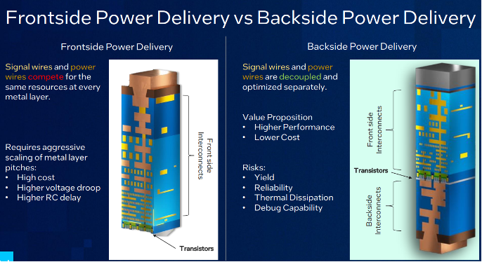
The transition to sub-2nm semiconductor nodes has revealed power delivery as the primary scaling bottleneck, not transistor physics itself. As interconnect resistance scales as ρL/A with decreasing wire cross-sectional area A, IR drop through traditional front-side power delivery networks threatens to halt Moore’s Law progression. Backside Power Delivery Networks (BSPDN) represent the industry’s response—a fundamental architectural shift that decouples power and signal routing domains to maintain voltage integrity at advanced nodes.
Physical Foundations and Scaling Challenges
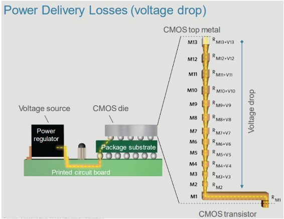
Traditional power delivery networks suffer from fundamental scaling limitations as feature sizes shrink. The power delivery impedance scales approximately as:
Z_PD ≈ ρL/A + jωL_parasitic
Where ρ is the metal resistivity, L is the interconnect length, and A is the wire cross-sectional area. At 2nm nodes, copper wire resistivity increases 2-3x due to electron surface scattering at narrow linewidths, while available routing area for power rails shrinks due to aggressive signal density requirements.
The IR drop problem becomes acute when power current density approaches the electromigration limit of ~2-5 MA/cm² for copper at operating temperatures. Traditional front-side networks force current through increasingly narrow via structures, creating reliability bottlenecks and voltage droop that can exceed 10% of VDD—far beyond acceptable limits for high-performance logic.
Foundry Implementation Strategies
TSMC N2 and N1.4 Roadmap
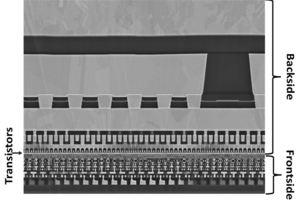
TSMC’s implementation for the N2 node (scheduled for 2025 production) employs a sophisticated wafer-level processing sequence. The approach begins with epitaxial growth of a SiGe etch-stop layer, typically 10-20nm thickness, followed by a thin silicon device layer.
After front-end transistor formation, the wafer undergoes temporary bonding to a carrier substrate using thermoplastic adhesives or direct oxide bonding. The critical thinning step employs chemical-mechanical planarization (CMP) to reduce the wafer thickness to less than 10μm, stopping precisely at the SiGe interface.
Nano through-silicon vias (nano-TSVs) with diameters under 100nm are then formed through several steps. First, backside surface passivation using atomic layer deposition (ALD) of Al₂O₃ or HfO₂. Next, via etching using reactive ion etching (RIE) with precise depth control. Then barrier layer deposition (TaN/Ta) to prevent copper diffusion. Finally, via filling with tungsten using chemical vapor deposition (CVD).
Intel PowerVia Architecture
Intel’s PowerVia technology, entering production on 18A, takes a different materials approach focused on buried power rail integration. Intel employs direct wafer bonding with Si-Si interface formation at approximately 1000°C, creating a more robust mechanical interface compared to adhesive-based approaches.
Their nano-TSV implementation uses aspect ratios greater than 10:1 with diameters approaching 50nm—pushing the limits of current tungsten gap-fill technology. Critical to Intel’s approach is the integration of embedded power rails within the buried oxide (BOX) layer of the bonded interface.
Samsung SF2Z Process Innovation
Samsung’s SF2Z process integrates BSPDN with their second-generation gate-all-around (GAA) nanosheet technology. Their approach emphasizes manufacturability, using larger via diameters (~80nm) to improve yield while maintaining adequate power delivery performance.
Samsung employs a hybrid copper-tungsten via fill strategy: copper for the bulk via fill with tungsten capping to prevent electromigration-induced voiding.
Materials Science and Interface Engineering
The BSPDN transition presents complex materials challenges that extend beyond conventional CMOS processing.
Bonding Interface Reliability
Direct silicon bonding creates Si-Si interfaces with bond energies approaching bulk silicon values. However, this requires precise surface preparation to achieve void-free bonding. Surface roughness must be controlled to sub-nanometer RMS levels, and particle contamination eliminated to prevent bonding defects that compromise mechanical integrity.
Thermal Stress Management
The bonded wafer stack experiences differential thermal expansion during processing and operation. With coefficient of thermal expansion (CTE) mismatch between Si and potential interlayer materials, thermal stress can exceed the fracture strength of thin silicon layers. Advanced process modeling using finite element analysis (FEA) is essential to optimize the thermal budget.
Via Fill Metallurgy
Nano-TSV filling presents unique challenges due to the high aspect ratio and nanoscale dimensions. Tungsten CVD using WF₆ precursors can suffer from pinch-off effects, creating voids that increase via resistance. Advanced fill strategies employ pulsed CVD or atomic layer deposition (ALD) nucleation layers to improve conformality.
Electrical Performance and Reliability Physics
BSPDN implementations must address fundamental reliability physics that become pronounced at advanced nodes.
Time-Dependent Dielectric Breakdown (TDDB)
The thin interlayer dielectrics in nano-TSVs experience high electric fields during operation. TDDB lifetime follows an exponential relationship with field strength, where advanced high-k dielectrics (HfO₂, Al₂O₃) with higher breakdown fields are essential for achieving 10-year reliability targets.
Electromigration in Nano-Conductors
Current density in nano-TSVs can approach 10 MA/cm², where electromigration becomes the dominant failure mechanism. The mean time to failure (MTTF) depends strongly on current density and temperature. Advanced barrier layers and via geometry optimization are critical for maintaining acceptable MTTF values.
Shot Noise and Power Integrity
At nanoscale dimensions, shot noise in the power delivery network becomes significant. This noise couples into the substrate and can affect sensitive analog circuits, requiring careful power delivery network design and decoupling strategies.
Manufacturing Integration and Yield Challenges
The transition to BSPDN introduces new yield loss mechanisms that require sophisticated process control.
Via Alignment Tolerance
Nano-TSV alignment to front-side contact structures requires overlay accuracy below 5nm across the full wafer. Advanced lithography alignment systems and computational overlay correction are essential to achieve this precision.
Wafer Warpage Control
The bonding and thinning processes can induce significant wafer warpage, which affects subsequent lithography steps. Active warpage compensation using backside pressure control and temperature profiling is necessary for high-yield manufacturing.
Metrology and Process Monitoring
Traditional electrical test methods are insufficient for nano-TSV characterization. Advanced techniques including scanning capacitance microscopy (SCM) and transmission electron microscopy (TEM) cross-sectioning are required for process development and yield learning.
Critical Analysis: Risks and Limitations
While BSPDN represents the current industry consensus for power delivery scaling, several critical limitations must be addressed.
Manufacturing Complexity and Cost
The additional processing steps significantly increase manufacturing complexity. Early industry estimates suggest cost increases, though exact figures remain proprietary. The yield learning curve for nano-TSV formation and wafer bonding could extend the technology’s economic viability timeline beyond current projections.
Alternative Technology Threats
Monolithic 3D integration technologies offer potential power delivery advantages without wafer bonding complexity, though they face thermal budget limitations for upper device layers. Advanced package-level power delivery through silicon interposers and embedded bridge technologies provide alternative paths, albeit with increased package complexity.
Thermal Management Trade-offs
Moving power delivery to the backside alters heat dissipation paths in ways that are not yet fully characterized in production environments. While theoretical models suggest benefits, real-world thermal performance in dense AI accelerator applications remains to be proven at scale.
Reliability Physics Uncertainties
The long-term reliability of nano-TSV structures under operational stress conditions lacks comprehensive data. Accelerated aging tests cannot fully capture all potential failure modes, particularly those involving interface degradation over 10+ year operational lifetimes.
Implications for AI and High-Performance Computing
BSPDN’s benefits align with AI accelerator requirements, particularly for large chips susceptible to IR drop issues due to size and high power density. The decoupled power delivery enables more aggressive power management strategies, including fine-grained power gating and dynamic voltage scaling optimized for AI workloads.
For materials science applications, BSPDN enables new compute architectures that were previously power-limited. Near-memory computing and neuromorphic architectures benefit from improved power delivery efficiency and reduced electrical interference between power and signal domains.
The technology’s maturation coincides with chiplet-based designs, where BSPDN can provide enhanced power delivery for heterogeneous integration scenarios combining logic, memory, and specialized accelerators.
Future Outlook and Research Directions
As BSPDN transitions from development to production, several research areas will determine its long-term viability.
Advanced Via Materials
Beyond tungsten, research into graphene nanoribbons and carbon nanotube via fills promises lower resistivity and improved electromigration resistance, though manufacturing scalability remains uncertain.
AI-Optimized Power Delivery
Machine learning-guided power delivery network design could optimize via placement and sizing for specific workload characteristics, potentially improving efficiency beyond current analytical design methods.
Quantum Effects
At sub-2nm dimensions, quantum tunneling through via barriers becomes significant, requiring new modeling approaches and potentially alternative materials strategies.
The successful implementation of BSPDN by 2025-2026 will determine whether the semiconductor industry can maintain its historical scaling trajectory or must pivot to alternative paradigms for performance improvement. The technology represents both the industry’s most ambitious manufacturing challenge and its best hope for continued scaling in the post-Moore’s Law era.
References
[1] L. Peters, “Backside Power Delivery Gears Up For 2nm Devices,” Semiconductor Engineering, Feb. 26, 2024. [Online]. Available: https://semiengineering.com/backside-power-delivery-gears-up-for-2nm-devices/
[2] S. K. Moore, “Intel Is All-In on Backside Power Delivery,” IEEE Spectrum, Jun. 8, 2023. [Online]. Available: https://spectrum.ieee.org/backside-power-delivery
[3] L. Peters, “Backside Power Delivery Nears Production,” Semiconductor Engineering, Apr. 17, 2025. [Online]. Available: https://semiengineering.com/backside-power-delivery-nears-production/
[4] S. K. Moore, “Intel 18A: A Peek at Intel’s Future Foundry Tech,” IEEE Spectrum, Feb. 21, 2024. [Online]. Available: https://spectrum.ieee.org/intel-18a
[5] L. Peters, “Challenges In Backside Power Delivery,” Semiconductor Engineering, Nov. 17, 2022. [Online]. Available: https://semiengineering.com/challenges-in-backside-power-delivery/
[6] L. Peters, “Backside Power Delivery Creates Fab Tool, Thermal Dissipation Barriers,” Semiconductor Engineering, Feb. 23, 2026. [Online]. Available: https://semiengineering.com/backside-power-delivery-creates-fab-tool-thermal-dissipation-barriers/
[7] L. Peters, “Big Changes Ahead In Power Delivery, Materials, And Interconnects,” Semiconductor Engineering, Mar. 22, 2023. [Online]. Available: https://semiengineering.com/big-changes-ahead-in-power-delivery-materials-and-interconnects/
[8] P. McLellan, “IEDM: Backside Power Delivery,” Semiconductor Engineering, Mar. 9, 2023. [Online]. Available: https://semiengineering.com/iedm-backside-power-delivery/
[9] L. Peters, “What’s Next For Through-Silicon Vias,” Semiconductor Engineering, Jan. 6, 2025. [Online]. Available: https://semiengineering.com/whats-next-for-tsvs/
[10] S. Wen, “The Other Side Of The Wafer: The Latest Developments In Backside Power Delivery,” Semiconductor Engineering, Feb. 16, 2023. [Online]. Available: https://semiengineering.com/the-other-side-of-the-wafer-the-latest-developments-in-backside-power-delivery/
[11] K. Heyman, “Backside Power Delivery Adds New Thermal Concerns,” Semiconductor Engineering, Mar. 14, 2024. [Online]. Available: https://semiengineering.com/backside-power-delivery-adds-new-thermal-concerns/
[12] M. LaPedus, “New Transistor Structures At 3nm/2nm,” Semiconductor Engineering, Jan. 25, 2021. [Online]. Available: https://semiengineering.com/new-transistor-structures-at-3nm-2nm/
This digest was generated by AaBot using real-time web and literature research.