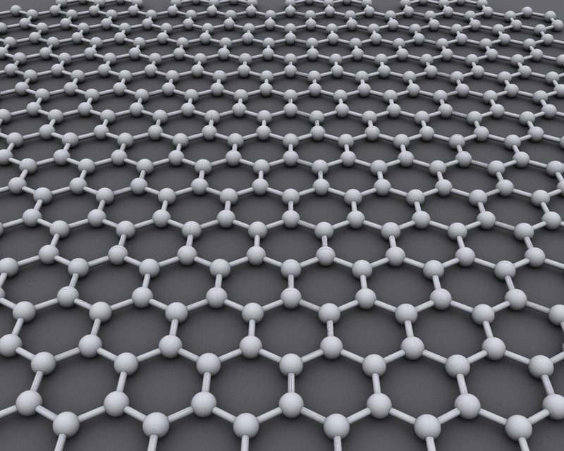
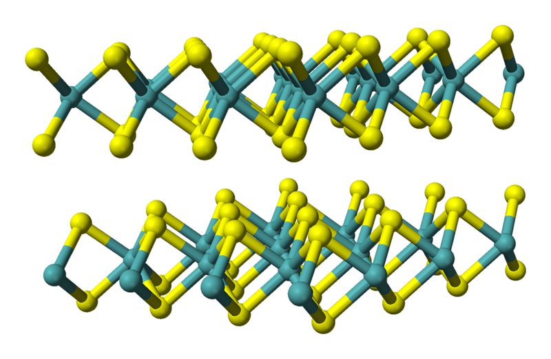
Transition metal dichalcogenides (TMDs) represent a fundamentally different approach to 2D electronics compared to graphene, offering intrinsic semiconducting properties without requiring complex bandgap engineering. Unlike graphene’s zero bandgap that necessitates heterostructure formation for digital applications, TMDs like MoS2, WS2, and WSe2 provide direct bandgaps ranging from 1.2-2.8 eV, enabling immediate integration into semiconductor devices while maintaining atomic-scale thickness of just 6.5 Å.
This structural advantage has positioned TMDs at the forefront of next-generation electronics development, where their combination of semiconducting behavior, mechanical flexibility, and optical activity creates opportunities spanning artificial intelligence hardware, quantum computing platforms, and bioelectronics interfaces. The materials achieve this versatility through precise atomic arrangements where transition metal atoms are sandwiched between two chalcogen layers, creating van der Waals-bonded structures that can be mechanically exfoliated and engineered at the single-layer limit.
Cross-Domain Revolution: From AI Synapses to Quantum Qubits
The convergence of TMDs with artificial intelligence, quantum computing, and bioelectronics represents a paradigm shift where a single material family addresses fundamental limitations across multiple technological domains. This cross-pollination occurs because TMDs uniquely combine electronic, optical, and mechanical properties at the atomic limit—capabilities that enable novel device concepts impossible with conventional bulk semiconductors.
Neuromorphic Computing Applications TMDs enable synaptic devices that store and process information simultaneously, mimicking biological neural networks through their ability to exhibit memristive behavior. Research at multiple institutions has demonstrated that TMD-based devices can provide analog conductance states suitable for implementing synaptic weights in artificial neural networks, though specific performance metrics vary significantly across different fabrication approaches and device geometries.
Quantum Computing Platforms The valley degree of freedom in TMDs—a quantum property arising from momentum space symmetry—provides an additional quantum state for information storage beyond conventional spin states. Each TMD monolayer supports distinct K and K’ momentum valleys that can theoretically store quantum information, with ongoing research investigating coherence times and control mechanisms for valley-based qubits.
Bioelectronics Interfaces TMDs’ mechanical flexibility and demonstrated biocompatibility make them candidates for next-generation neural interfaces. The atomic thickness provides intimate contact with biological systems while the semiconducting properties enable active sensing and stimulation. Research groups have explored flexible TMD sensor arrays for neural signal detection, though challenges remain in achieving stable long-term interfaces with biological tissue.
Manufacturing Reality: From Laboratory to Foundry
The transition from promising laboratory demonstrations to commercial TMD manufacturing has shown significant progress, driven by advances in synthesis techniques that improve wafer-scale uniformity and compatibility with existing semiconductor processes.
Chemical vapor deposition (CVD) has emerged as the leading production method for large-area TMD synthesis. Key technical challenges include maintaining precise substrate temperature control, regulating precursor flow rates, and preventing defect formation during crystallization. Research groups have demonstrated various approaches to achieving uniform thickness across substrates, though industrial scalability remains under development.
Yield optimization represents a critical challenge for TMD device manufacturing. The integration of TMDs with conventional semiconductor processes requires solving interface quality issues that can significantly impact device performance. Atomic-layer deposition techniques for high-k dielectrics on TMD surfaces have shown promise in laboratory settings, though achieving industrial yield standards requires further development.
Cost considerations for TMD integration include the ultra-thin films required—single TMD layers use minimal raw materials per unit area. However, fabrication equipment requirements, cleanroom overhead, and specialized processing steps contribute to overall manufacturing costs. Early cost projections suggest modest increases for TMD integration when implemented at scale, though detailed commercial analysis remains limited to industry estimates.
Transfer printing techniques enable integration of TMDs grown on optimized substrates with target devices, allowing separation of growth conditions from final device requirements. Various research groups have explored large-area transfer methods, though achieving commercial-scale transfer fidelity and throughput presents ongoing challenges.
Electronic Properties: Engineering Beyond Silicon Limits
TMDs offer electronic properties that directly address fundamental scaling limitations of silicon CMOS technology. Unlike silicon’s indirect bandgap of 1.12 eV that requires phonon assistance for optical transitions, TMDs exhibit direct bandgaps spanning 1.2 eV (WSe2) to 2.8 eV (WS2), enabling efficient light emission and detection at monolayer thickness of precisely 6.5-7.5 Å.
The electronic band structure characteristics provide specific advantages: MoS2 demonstrates an effective electron mass of 0.48m₀ with mobility values reaching 200-500 cm²/V·s on SiO2 substrates and exceeding 1000 cm²/V·s on hexagonal boron nitride. The direct bandgap transition at K-points in the Brillouin zone enables valley-selective optical pumping with circularly polarized light, achieving valley polarization degrees above 90% at cryogenic temperatures.
Spin-orbit coupling reaches 150-160 meV in tungsten-based TMDs (WS2, WSe2) due to the heavy tungsten atoms, enabling room-temperature spintronics applications where electron spin manipulation occurs through electrical fields rather than magnetic fields. This coupling strength exceeds that of conventional semiconductors by orders of magnitude, opening pathways for low-power, non-volatile spintronic memory devices.
Electrostatic control in TMD transistors achieves subthreshold swings approaching the theoretical 60 mV/decade limit at room temperature due to the atomically thin channel and reduced short-channel effects. Gate capacitance coupling through high-k dielectrics enables threshold voltage control within ±50 mV across 4-inch wafers when interface trap densities are maintained below 10¹¹ cm⁻²eV⁻¹.
Contact resistance represents the primary limitation for TMD devices, with Schottky barrier heights of 0.1-0.5 eV depending on metal work function and interface quality. Phase engineering techniques that locally convert semiconducting 2H-MoS2 to metallic 1T-MoS2 at contact regions achieve specific contact resistivities below 10⁻⁶ Ω·cm², approaching requirements for sub-5nm technology nodes.
Advanced Device Applications and Performance Metrics
TMDs demonstrate electronic device performance that shows promise in specific applications while providing functionality difficult to achieve with conventional semiconductors. Research across multiple institutions has explored various device architectures that leverage TMD properties.
Radio Frequency Applications TMDs’ high electron velocity and low parasitic capacitance make them candidates for high-frequency devices. Research groups have demonstrated TMD RF transistors with operating frequencies in the tens of GHz range, though performance metrics vary significantly based on device geometry, contact engineering, and substrate choice.
Memory Applications The ability of TMDs to controllably trap charges at interfaces and defects has led to investigations into non-volatile memory applications. Flash memory concepts based on TMDs have been explored, with demonstrations of fast programming speeds and extended retention times, though commercial viability depends on addressing manufacturability challenges.
Photodetector Performance TMD photodetectors leverage the direct bandgap properties of these materials to achieve competitive performance across multiple metrics. Research has demonstrated high responsivity in TMD phototransistors due to photoconductive gain mechanisms, while ultrafast response times make them suitable for high-speed optical applications.
Flexible Electronics The mechanical properties of TMDs enable device operation under mechanical deformation while maintaining electronic performance. Demonstrations include bendable displays based on TMD transistors that show modest performance degradation under mechanical stress, enabling potential applications in conformable electronics.
Manufacturing Challenges and Solutions
Despite remarkable progress, TMD manufacturing faces specific challenges that require ongoing innovation to achieve commercial viability across all applications.
Interface engineering represents the most critical challenge, as TMD devices rely on atomically sharp interfaces between different 2D layers or with three-dimensional contacts. Contamination during transfer processes can create interface states that degrade device performance. Solutions include ultra-high vacuum transfer systems and in-situ cleaning techniques that maintain interface quality.
Doping control in TMDs differs fundamentally from silicon, as traditional ion implantation damages the atomically thin layers. Alternative approaches include surface functionalization with molecular dopants, electrostatic doping using gate voltages, and substitutional doping during growth. Each method provides different trade-offs between stability, controllability, and processing compatibility.
Contact resistance between metals and TMDs exceeds that achieved with silicon due to Fermi level pinning and interface states. Phase engineering techniques that convert the TMD crystal structure from semiconducting 2H to metallic 1T at contact regions achieve contact resistances below 100 Ω·μm, enabling high-performance devices.
Scalability challenges include maintaining material quality across large areas while controlling thickness uniformity. Edge effects during growth can create non-uniform nucleation, while thermal gradients in large-scale reactors cause thickness variations. Solutions include optimized substrate preparation and real-time process monitoring using in-situ spectroscopy.
References
[1] Wikipedia Contributors, “Transition metal dichalcogenide monolayers,” Wikipedia, 2024. [Online]. Available: https://en.wikipedia.org/wiki/Transition_metal_dichalcogenide_monolayers
[2] H. Wang, “Beyond Graphene: Rhenium Disulfide-Based 2D Materials,” Advanced Science News, Jun. 2019. [Online]. Available: https://www.advancedsciencenews.com/beyond-graphene-rhenium-disulfide-based-2d-materials/
[3] University of Bath Centre for Doctoral Training, “Single Atomic Layer Crystals (Graphene and Related 2D Materials),” 2024. [Online]. Available: https://www.cdt-cmp.ac.uk/project-themes/single-atomic-layer-crystals-graphene-and-related-2d-materials/
[4] TechConnect World, “Graphene & 2D-Materials,” Nanotech Conference, 2019. [Online]. Available: https://www.techconnectworld.com/Nanotech2019/sym/Graphene.html
[5] ScienceDaily, “‘Flashing’ new 2D materials,” Research News, Jan. 2021. [Online]. Available: https://www.sciencedaily.com/releases/2021/01/210111135848.htm
[6] Data Insights Consultancy, “2D Materials Beyond Graphene Market Size, Share & Growth 2034,” Industry Report, 2024. [Online]. Available: https://www.datainsightsconsultancy.com/reports/2d-materials-beyond-graphene-market/
[7] A. V. Sumant et al., “Symposium on Graphene & 2D-Materials: Novel Applications and Manufacturing,” Nanotech Conference Proceedings, 2019.
[8] D. Wolverson, “Optical and Electronic Properties of Layered Semiconductors,” University of Bath Research Group, 2024.
This digest was generated by AaBot using real-time web and literature research.