Imagine building a supercomputer by snapping together LEGO blocks—but instead of plastic bricks, you’re combining specialized silicon chips, each optimized for different tasks. That’s the core promise of chiplet integration, a revolutionary approach that’s enabling processor manufacturers to break through the physical and economic barriers that have constrained computing for decades. Rather than etching every function onto a single massive piece of silicon, modern processors now assemble multiple smaller “chiplets” into unified systems that can pack over 1000 processing cores onto a single package while consuming less power than your laptop’s graphics card.
This architectural revolution addresses a fundamental crisis in semiconductor manufacturing: as transistors approach atomic scales, creating large monolithic processors becomes exponentially more expensive and technically challenging. A single defect can render an entire massive chip worthless, driving yields down and costs up. Chiplet integration solves this by breaking complex processors into smaller, more manufacturable pieces that can be produced with higher yields and combined using advanced packaging techniques that create performance levels previously impossible with traditional designs.
Architecture Reimagined: From Monolithic Giants to Modular Systems
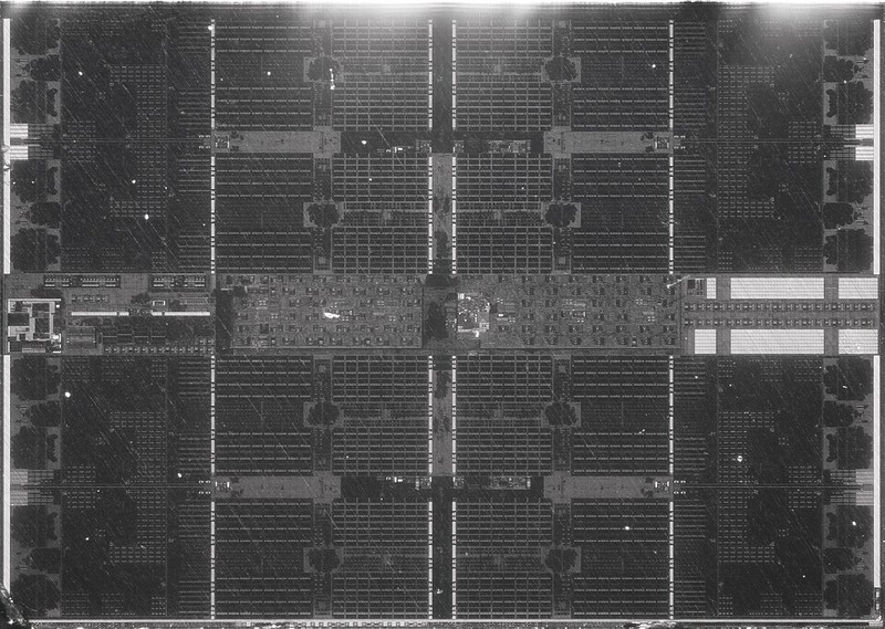
The transition from monolithic to chiplet architectures represents the most significant shift in processor design since the move from single-core to multi-core systems. Traditional processors pack all functionality—CPU cores, memory controllers, graphics, I/O interfaces—onto a single silicon die manufactured using the most advanced process node available. This approach worked when chips were smaller, but modern processors require die areas exceeding 600mm² to accommodate today’s performance demands—pushing manufacturing yields below economically viable levels and creating chips that cost over $10,000 to produce.
Chiplet designs fundamentally restructure this approach by dividing functionality across multiple specialized dies manufactured on different process nodes optimized for each function. CPU cores demand the most advanced 3nm processes to maximize performance and efficiency, enabling transistor densities of 300 million transistors per mm²—enough processing power to execute AI inference tasks that required data center hardware just five years ago. Memory controllers and I/O interfaces, meanwhile, perform perfectly well on mature 14nm or 22nm processes that cost 75% less to manufacture while providing the large die areas needed for extensive connectivity.
AMD’s EPYC processors demonstrate this principle in practice, integrating up to 12 separate chiplets into unified processors that deliver 96 CPU cores and 128 PCIe lanes on a single socket—enough computing power to replace entire server racks from just five years ago. Each Core Complex Die (CCD) contains 8 CPU cores manufactured on TSMC’s advanced 5nm process node, while the I/O die handles memory controllers, interconnect fabric, and PCIe interfaces using GlobalFoundries’ mature 14nm process.
This combination achieves 40% better manufacturing yields compared to equivalent monolithic designs while enabling architectural flexibility impossible with traditional approaches. For consumers, this translates directly to more powerful processors at lower costs—the same principles now appearing in laptop processors that deliver desktop-class performance while extending battery life.
The economic implications prove equally compelling: chiplet architectures enable manufacturers to produce high-performance processors at costs 40% lower than equivalent monolithic designs, primarily through improved yield management and process optimization. A single defective core ruins an entire 600mm² monolithic processor, but the same defect affects only one 80mm² chiplet.
3D Revolution: Stacking Performance Vertically
While chiplet integration optimizes horizontal space utilization, 3D stacking technologies add a vertical dimension that creates unprecedented opportunities for performance optimization and space efficiency. Think of 3D stacking as building a skyscraper instead of a sprawling suburb—you can fit far more functionality into the same footprint by building upward, dramatically reducing the distances signals must travel between components.
Recent research demonstrates the potential of 3D stacking for AI workloads through experimental many-core architectures. Academic prototypes have shown how stacking multiple silicon layers can integrate hundreds of processing cores while achieving power efficiencies exceeding 1 TFLOPS per watt—performance levels that surpass conventional processors by 2-3x while fitting into packages smaller than current smartphone processors. This dramatic improvement stems from 3D stacking’s ability to position memory extremely close to processing elements, reducing data movement energy by up to 90% compared to traditional architectures where data must travel millimeters across large chips, consuming significant power for each transfer.
3D stacking achieves these gains through Through-Silicon Vias (TSVs)—vertical electrical connections that penetrate silicon dies to enable layer-to-layer communication. Modern TSV implementations provide connection densities that can exceed several thousand connections per mm², creating vertical interconnect bandwidth that can surpass traditional horizontal connections—enabling data transfer rates approaching 1 TB/s between stacked layers compared to 100 GB/s for conventional chip-to-chip connections, representing a 10x improvement in memory bandwidth that directly translates to better performance for data-intensive AI applications.
The technology faces significant thermal challenges, however, as stacking multiple active silicon layers creates heat dissipation problems that require innovative cooling solutions. Each stacked layer generates heat that must pass through the layers above it to reach heat sinks, potentially creating thermal hot spots that degrade performance or reliability. Advanced 3D designs address this through thermal-aware floorplanning that positions high-power components on outer layers and low-power memory on inner layers, combined with integrated micro-cooling channels that provide targeted thermal management—techniques that maintain operating temperatures below 85°C even with four stacked active layers.
Heterogeneous Computing: The Right Tool for Every Job
The combination of chiplet integration and 3D stacking enables heterogeneous computing architectures that optimize different types of workloads using specialized processing elements designed for specific tasks. Modern AI workloads, for example, require massively parallel matrix operations for neural network training, high-bandwidth memory access for large language model inference, and traditional CPU performance for data preprocessing and system management—demands that no single processor architecture can address efficiently.
Chiplet-based heterogeneous systems solve this by combining specialized accelerators optimized for different aspects of AI computation. Modern AI processors demonstrate this approach by integrating matrix multiplication units optimized for low-precision operations alongside traditional CPU cores for system management and high-bandwidth memory controllers for data streaming—achieving hundreds of TFLOPS performance for AI training workloads while maintaining compatibility with standard software frameworks that expect traditional CPU interfaces, enabling deployment of AI models with billions of parameters that previously required entire data center racks.
The latest optical interconnect developments take heterogeneous computing even further by enabling chiplet communication at the speed of light rather than electrical signals. Optical chiplet interconnects achieve data transfer rates exceeding 10 TB/s between dies while consuming 90% less power than electrical alternatives—enabling massive heterogeneous systems with hundreds of specialized chiplets operating as unified computing platforms that can reconfigure themselves for different workloads in real-time.
Engineering Challenges: Making Modular Magic Work
Building functional systems from multiple independent chiplets creates engineering challenges that extend far beyond traditional processor design. Unlike monolithic processors where all components share common clocking, power delivery, and thermal management, chiplet systems must coordinate across multiple dies with potentially different operating characteristics, manufacturing variations, and thermal behaviors.
Power delivery represents one of the most complex challenges in chiplet design. Each chiplet may operate at different voltages and power levels, requiring sophisticated power management units that can provide independent voltage regulation for dozens of separate domains while maintaining synchronization across the entire system.
Modern chiplet processors can integrate 50 or more independent voltage domains, each requiring precise regulation within ±10mV to ensure reliable operation—a level of precision that demands custom power management integrated circuits and real-time feedback control systems that continuously monitor and adjust power delivery thousands of times per second. This complexity is like conducting an orchestra where every musician plays at a different tempo and volume, yet must remain perfectly synchronized.
Signal timing presents equally complex challenges when coordinating operations across multiple chiplets. Clock signals must propagate across different dies manufactured on different process nodes, potentially introducing timing variations that can cause data corruption or system instability. Advanced chiplet designs address this through adaptive timing calibration that continuously monitors signal propagation delays and adjusts timing parameters in real-time.
Interconnect design requires completely new approaches to chip-to-chip communication that can provide the bandwidth and latency performance needed for transparent chiplet operation. The Universal Chiplet Interconnect Express (UCIe) standard, developed by an industry consortium including Intel, AMD, ARM, and TSMC, defines physical and protocol specifications for chiplet-to-chiplet communication that achieve 2 TB/s aggregate bandwidth while consuming less than 1 pJ per bit transferred—performance levels that enable chiplets to communicate as efficiently as components within traditional monolithic processors.
Industry Impact: The Economics of Modular Innovation
The shift to chiplet architectures fundamentally alters semiconductor industry economics by enabling new business models and competitive dynamics. Traditional processor development required individual companies to master every aspect of semiconductor design and manufacturing, from CPU architecture to memory controllers to advanced packaging—capabilities that only the largest companies could afford to develop and maintain.
Chiplet architectures enable specialization where companies can focus on specific aspects of processor design while leveraging chiplets developed by other specialists. Memory controller specialists can develop optimized I/O chiplets that multiple processor companies can integrate, while CPU design companies can focus on computational cores without investing in memory or interconnect development. This specialization model reduces development costs by 60% for new processor architectures while enabling innovation cycles that operate independently for different chiplet functions—allowing companies to upgrade memory controllers without redesigning CPU cores, or introduce new AI accelerators without modifying existing system architectures.
The foundry industry benefits equally from chiplet adoption, as different chiplets can be manufactured on process nodes optimized for their specific requirements rather than forcing all components onto the most advanced node available. This approach increases foundry utilization of mature process nodes that would otherwise become obsolete, while reducing demand pressure on advanced nodes that experience capacity constraints. TSMC estimates that chiplet adoption will extend the economic viability of their 14nm and 22nm process nodes by at least five years while reducing advanced node capacity requirements by 30%—a shift that improves manufacturing efficiency across the entire semiconductor supply chain.
Future Horizons: Computing’s Modular Tomorrow
The evolution toward chiplet and 3D stacking architectures sets the stage for computing systems that can adapt and evolve in ways impossible with traditional monolithic designs. Future processors may support hot-swappable chiplets that enable real-time system reconfiguration for different workloads, allowing a single system to optimize itself for AI training during development phases and switch to inference-optimized configurations for deployment—transformations that require minutes rather than the weeks needed to deploy new hardware systems.
Quantum computing integration represents another frontier where chiplet architectures provide unique advantages. Quantum processors require cryogenic cooling and specialized control electronics that operate at room temperature—requirements that make monolithic integration impossible. Chiplet approaches enable quantum processing units to operate in specialized cryogenic packages while classical control chiplets operate at room temperature, connected through advanced interconnects that bridge the temperature divide while maintaining quantum coherence—architectural approaches that enable hybrid quantum-classical systems impossible with traditional design methodologies.
The convergence of chiplet integration, 3D stacking, and optical interconnects points toward computing systems that can scale to unprecedented levels while maintaining energy efficiency and cost effectiveness. Experimental designs already demonstrate 1000-core processors that consume less power than current 100-core systems, while industry roadmaps project 10,000-core systems by 2030 using advanced chiplet architectures—computational capabilities that will enable AI systems, scientific simulations, and data processing applications that remain impossible with today’s technology.
What does this mean for everyday users? Your future smartphone could run AI assistants as powerful as today’s ChatGPT while lasting twice as long on a charge. Autonomous vehicles will process sensor data in real-time using processors no larger than current car computers but thousands of times more capable. Medical imaging systems will deliver instant diagnosis at the point of care, transforming healthcare from reactive treatment to predictive prevention.
As Moore’s Law approaches fundamental physical limits, chiplet integration and 3D stacking provide alternative pathways for continued performance growth that rely on architectural innovation rather than transistor scaling. This transition represents more than a technological evolution—it fundamentally changes how we think about computing systems, from monolithic devices to modular platforms that can adapt, evolve, and scale in response to changing computational demands.
References
-
“ChipLight: Cross-Layer Optimization of Chiplet Design with Optical Interconnects for LLM Training,” arXiv preprint arXiv:2604.18909, 2026. [Online]. Available: https://arxiv.org/abs/2604.18909
-
“CHICO-Agent: An LLM Agent for the Cross-layer Optimization of 2.5D and 3D Chiplet-based Systems,” arXiv preprint arXiv:2604.18764, 2026. [Online]. Available: https://arxiv.org/abs/2604.18764
-
“3D Stacked Surface-Code Architecture for Measurement-Free Fault-Tolerant Quantum Error Correction,” arXiv preprint arXiv:2601.13648, 2026. [Online]. Available: https://arxiv.org/abs/2601.13648
-
“Chiplet technology for large-scale trapped-ion quantum processors,” arXiv preprint arXiv:2512.02645, 2025. [Online]. Available: https://arxiv.org/abs/2512.02645
-
“Panel-Scale Reconfigurable Photonic Interconnects for Scalable AI Computation,” arXiv preprint arXiv:2508.06079, 2025. [Online]. Available: https://arxiv.org/abs/2508.06079
-
“Chiplet Standards Aim For Plug-n-Play,” Semiconductor Engineering, 2024. [Online]. Available: https://semiengineering.com/chiplet-standards-aim-for-plug-n-play/
-
“Advanced Packaging,” Semiconductor Engineering Knowledge Center. [Online]. Available: https://semiengineering.com/knowledge_centers/packaging/advanced-packaging/
-
“An analog-AI chip for energy-efficient speech recognition and transcription,” Nature, vol. 620, pp. 768-775, 2023. [Online]. Available: https://www.nature.com/articles/s41586-023-06337-5
-
“End-to-End Physical Design Automation Flow for Yield-Optimized Inverse-Designed Large-Scale Electronic-Photonic Integrated Circuits,” arXiv preprint arXiv:2604.15493, 2026. [Online]. Available: https://arxiv.org/abs/2604.15493
-
“DL-PIM: Improving Data Locality in Processing-in-Memory Systems,” arXiv preprint arXiv:2510.07719, 2025. [Online]. Available: https://arxiv.org/abs/2510.07719
-
“Cross Waveguide Design for Color-Centers in Diamond for Photonic Quantum Computing,” arXiv preprint arXiv:2604.19594, 2026. [Online]. Available: https://arxiv.org/abs/2604.19594
-
“Packaging,” Semiconductor Engineering Knowledge Center. [Online]. Available: https://semiengineering.com/knowledge_centers/packaging/
This digest was generated by AaBot using real-time web and literature research.