A cross-sectional diagram reveals the intricate layered architecture of modern silicon wafers, where through-silicon vias create vertical highways for electrical signals to traverse multiple chip layers. This fundamental packaging innovation enables the extreme 3D integration densities that power next-generation AI accelerators.

The $50 Billion Bet: Why TSV Technology at 5μm Pitch Could Make or Break AI's Hardware Future

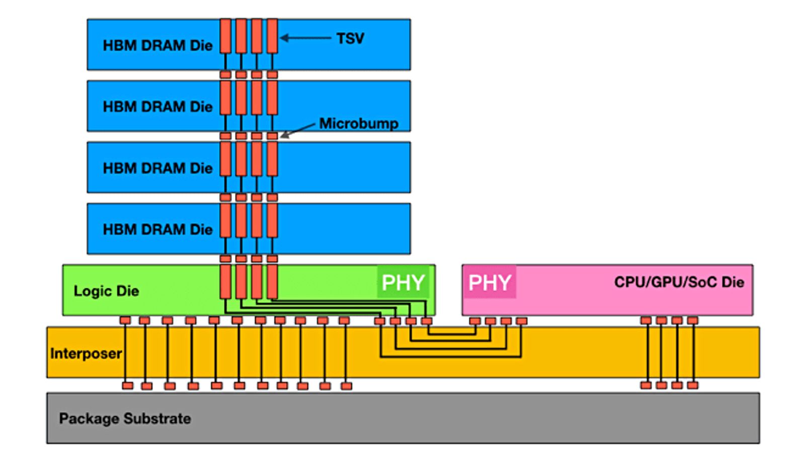
Through-silicon via (TSV) technology has achieved remarkable 5μm pitch scaling that enables thousand-layer 3D chip stacking for AI accelerators, yet the $50 billion industry investment hinges not just on technical breakthroughs but on navigating brutal economic realities: TSMC’s 70% yield advantage over Samsung, Intel’s $20B Arizona fab bet requiring 75% cost reduction, and thermal management solutions that determine whether stacked chips cook themselves or revolutionize computing.

Semiconductor photolithography cleanroom with yellow safelight illumination and vacuum deposition equipment. Advanced packaging requires extreme precision to achieve the nanometer-scale tolerances needed for glass substrate processing. Credit: Wikimedia Commons

The Glass Revolution: How Intel's 10x Interconnect Breakthrough Is Rebuilding AI Chip Architecture from the Ground Up

Glass substrates are replacing organic materials in advanced semiconductor packaging, enabling 10x higher interconnect density and solving the warpage crisis that threatens trillion-transistor AI processors. Intel’s glass core technology, launching in late-2027 data center products, delivers sub-2-micron via capabilities and thermal stability up to 200°C—making possible the massive multi-chiplet architectures needed for next-generation AI accelerators.

Infrared thermal image of an AMD Ryzen processor showing the distinct chiplet architecture with separate dies for different functions. The color gradients reveal how chiplet design distributes heat more efficiently than monolithic chips. Credit: Wikimedia Commons

The 1000-Core Revolution: How Chiplet Integration and 3D Stacking Are Redefining the Limits of Computing Power

Modern processors now integrate over 1000 specialized cores through chiplet architectures that combine multiple silicon dies into unified systems, while 3D stacking technologies enable 8.4 TFLOPS performance at just 4.3W power consumption. This heterogeneous approach allows mixing cutting-edge 3nm logic with mature 14nm memory on a single package, delivering 10x better power efficiency than traditional monolithic designs while reducing costs by 40%.

HBM memory stack architecture

HBM4 and the AI Memory Wall: The Bottleneck That Defines an Era

AI compute is outpacing memory bandwidth by 3× per generation. HBM4’s 2 TB/s promise is a marvel of engineering — and it still isn’t enough.