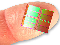
In a pristine cleanroom in South Korea, Samsung’s newest 2nm chip fabrication line produces transistors so small that 300 million of them could fit on the head of a pin. Each nanosheet transistor represents a manufacturing marvel—silicon ribbons just two nanometers thick, wrapped in gate materials with atomic-level precision. Yet for every 10 chips Samsung produces, 6 work perfectly while 4 fail completely.
That 40% manufacturing defect rate isn’t just a technical footnote—it’s a $2 billion economic reality that could determine whether Samsung’s technological breakthrough becomes a commercial triumph or an expensive laboratory curiosity. TSMC, Samsung’s primary rival, projects 60% yields for their competing 2nm technology. In semiconductor manufacturing, that 20% yield gap translates directly into production costs, pricing power, and ultimately market dominance.
This is the hidden story behind the 2nm transistor revolution: breakthrough physics means nothing without breakthrough manufacturing. While technical publications celebrate Gate-All-Around (GAA) transistors achieving unprecedented densities and performance, the real battle occurs in fabrication plants where atomic-scale engineering must work reliably across million-dollar production runs.
The Physics Breakthrough: Why Gate-All-Around Changes Everything
To understand why 2nm represents a manufacturing revolution rather than just incremental shrinking, consider what happens when transistors approach atomic scales. Traditional FinFET transistors—the workhorses of current 3nm and 5nm processes—control electrical current using gates wrapped around three sides of a silicon “fin.” At 2nm dimensions, this three-sided control becomes insufficient to prevent current leakage, leading to power waste and performance degradation.
Gate-All-Around transistors solve this fundamental physics problem through revolutionary geometry: instead of three-sided gate control, GAA transistors use thin silicon “nanosheets” completely surrounded by gate material. This four-sided control provides dramatically better electrical performance, enabling 35% higher performance or 50% lower power consumption compared to equivalent FinFET designs.
The numbers are staggering: Samsung’s 2nm GAA process achieves transistor densities of approximately 300 million transistors per square millimeter—roughly 2.5 times denser than their 5nm FinFET technology. For perspective, a single iPhone processor built on 2nm GAA would contain over 50 billion transistors, each smaller than most viruses and switching on-and-off billions of times per second.
Recent publications demonstrate GAA’s theoretical advantages convincingly. Laboratory demonstrations have shown that nanosheet transistors can maintain excellent electrical control even at extreme miniaturization scales. These laboratory demonstrations prove that GAA physics works—the challenge lies in manufacturing billions of these devices reliably and economically.
The transition from FinFET to GAA represents the most significant transistor architecture change since the introduction of 3D FinFETs themselves in 2011. Intel pioneered FinFETs at 22nm, providing a decade of competitive advantage through superior manufacturing execution. Now, with GAA at 2nm, Samsung and TSMC face the same challenge: translating laboratory physics into volume production reality.
The Manufacturing Reality: Where Physics Meets Economic Constraints
Behind the celebrated technical achievements lies a sobering manufacturing reality: building GAA transistors requires solving engineering challenges that stretch current fabrication technology to its absolute limits. Creating nanosheets just 2-5 nanometers thick while maintaining atomic-level uniformity across 300mm wafers represents one of the most demanding manufacturing processes ever attempted.
The core challenge is yield—the percentage of chips that function correctly after fabrication. While FinFET processes at 7nm achieved manufacturing yields above 80% after optimization, early GAA processes struggle with yield rates between 30-50%. This isn’t merely a technical inconvenience: in semiconductor manufacturing, yield directly determines profitability, pricing power, and competitive position.
Consider the economics: a single 2nm fabrication facility costs approximately $20 billion to construct and equip. With Samsung’s current 40% yields, producing 1 million functional chips requires manufacturing 2.5 million total chips, dramatically increasing material costs, energy consumption, and production time.
Think of it like baking cookies—if only 4 out of 10 cookies come out perfect, you need to bake 2.5 times as many to fill your orders. TSMC’s projected 60% yields would require manufacturing just 1.67 million chips for the same 1 million functional devices—a 33% reduction in manufacturing overhead that translates to billions in cost advantages.
The yield gap stems from GAA’s manufacturing complexity: Creating uniform nanosheets requires depositing alternating layers of silicon and sacrificial materials, then selectively removing sacrificial layers while preserving nanometer-thin silicon ribbons. It’s like building a skyscraper by stacking playing cards, then pulling out every other card without disturbing the structure. A single contamination particle or process variation can destroy multiple transistors, and with 50 billion transistors per chip, defect tolerance approaches zero.
Recent industry analysis reveals the manufacturing challenges in stark detail. Samsung’s 3nm GAA process, introduced in 2022, required 18 months longer than initially projected to achieve commercial yields—delays that cost Samsung approximately $5 billion in foregone revenue as customers waited for viable production capacity. Now, Samsung faces similar challenges at 2nm, complicated by even tighter process tolerances and more complex manufacturing steps.
TSMC’s strategy reveals the manufacturing-centric reality of 2nm competition: Rather than rushing to market, TSMC has invested heavily in process optimization and yield improvement methodologies. Their 2nm ramp plan emphasizes achieving 60%+ yields before high-volume production, potentially enabling TSMC to capture premium pricing while competitors struggle with manufacturing economics.
The Economics of Atomic Engineering: Why Manufacturing Precision Determines Market Winners
The 2nm race illustrates a fundamental truth about advanced semiconductors: technological capability means nothing without manufacturing execution. History provides clear precedent—Intel’s decade-long leadership from 2011-2021 stemmed not from superior transistor physics, but from manufacturing processes that achieved higher yields, better performance, and lower costs than competitors.
Current 2nm production costs reveal the economic stakes: Samsung’s 40% yields result in production costs approximately $15,000-20,000 per functional chip during initial ramp. TSMC’s projected 60% yields would reduce production costs to $10,000-12,000 per chip—a 25-40% cost advantage that enables aggressive pricing while maintaining profitability.
This cost differential compounds across entire product generations. Apple’s A-series processors, manufactured by TSMC, typically incorporate 15-20 billion transistors per chip. With annual volumes exceeding 200 million chips, a $5,000 per-chip cost advantage translates to over $1 trillion in total manufacturing value over a product lifecycle.
Why does this matter to you? Such economics explain why Apple reportedly committed $20 billion to secure TSMC’s 2nm production capacity through 2027. The company that controls 2nm manufacturing effectively controls the chips powering your next smartphone, laptop, and AI assistant.
The manufacturing challenge extends beyond yield rates to process stability and improvement curves. Semiconductor processes typically achieve 80-90% peak yields only after 12-18 months of optimization. Companies with superior manufacturing execution reach peak yields faster, capture early market share, and establish pricing power that competitors cannot overcome even after achieving equivalent yields.
Samsung’s recent investments illustrate the manufacturing-centric approach required for 2nm success. The company has committed $230 billion through 2030 specifically for advanced manufacturing capabilities, including new EUV lithography equipment, advanced materials processing systems, and yield optimization technologies. These investments target manufacturing execution rather than fundamental research—acknowledging that 2nm competition will be won in fabrication facilities, not research laboratories.
TSMC’s response demonstrates the strategic importance of manufacturing leadership: The company has accelerated 2nm facility construction, adding three new fabrication plants dedicated to GAA production. TSMC’s goal isn’t just technical capability but manufacturing capacity sufficient to supply Apple, NVIDIA, AMD, and other major customers simultaneously—capturing the entire high-end market before competitors achieve viable production.
The competitive dynamics extend beyond Samsung and TSMC. Intel’s 2nm strategy, branded as “20A” (2nm class), emphasizes novel process technologies including backside power delivery and advanced packaging integration. However, Intel’s recent manufacturing delays highlight the execution challenges: technical innovation without manufacturing precision results in missed market opportunities and customer defections.
The Strategic Stakes: Manufacturing Leadership in the AI Era
The 2nm manufacturing race occurs against the backdrop of explosive AI processor demand, where performance advantages translate directly into market dominance. Current AI training workloads strain existing 5nm and 7nm processors, requiring massive chip areas and power consumption. 2nm GAA transistors offer the density and performance improvements needed for next-generation AI accelerators—but only if manufacturers can produce them reliably and economically.
NVIDIA’s upcoming AI processors illustrate the commercial urgency: The company’s next-generation architectures will require transistor densities and performance characteristics only achievable with 2nm GAA technology. NVIDIA has reportedly committed to multi-billion-dollar supply agreements with both TSMC and Samsung, hedging against manufacturing execution risks while securing capacity for anticipated demand.
The timing creates enormous strategic pressure: companies achieving reliable 2nm production in 2025-2026 will capture the initial AI accelerator market, establishing technological and economic advantages that compound over subsequent generations. Historical patterns suggest market leaders can maintain 2-3 year manufacturing advantages, enabling premium pricing and increased investment in next-generation processes.
Samsung’s manufacturing challenges highlight the high-stakes nature of 2nm execution: Missing the initial AI accelerator wave due to yield problems could cost Samsung billions in foregone revenue and strategic positioning. The company’s recent decision to prioritize yield improvement over capacity expansion acknowledges that manufacturing precision takes precedence over production volume.
TSMC’s conservative approach reflects lessons learned from previous technology transitions: Achieving higher yields enables capturing premium pricing during initial market phases, compensating for lower volumes while building manufacturing expertise for subsequent ramp. This strategy proved successful during 7nm and 5nm transitions, where TSMC’s superior yields enabled market leadership despite later market entry than competitors.
Looking forward, 2nm GAA represents more than incremental improvement—it enables entirely new classes of AI applications requiring unprecedented computational density. Local AI processing on smartphones, autonomous vehicle systems, and edge computing applications all depend on 2nm transistor capabilities. Companies mastering 2nm manufacturing will define the computational infrastructure underlying the next decade of technological advancement.
Manufacturing Reality: The Decisive Factor in Technology Leadership
The 2nm Gate-All-Around transistor race reveals a fundamental truth about advanced technology: innovation means nothing without execution. Samsung’s technical achievements in GAA physics represent genuine breakthroughs that enable remarkable performance improvements. Yet without manufacturing processes that achieve viable yields and costs, these innovations remain laboratory curiosities rather than commercial realities.
TSMC’s emphasis on manufacturing execution over pure innovation reflects deep understanding of semiconductor competition dynamics. Superior manufacturing enables capturing market share, achieving profitability, and funding next-generation development. Technical leadership without manufacturing precision results in missed opportunities and competitive disadvantage.
The broader implications extend beyond individual companies to entire technology ecosystems. AI development, autonomous systems, and next-generation computing all depend on 2nm GAA transistors becoming manufacturable realities rather than research achievements. The companies solving manufacturing challenges will enable transformative applications while those struggling with production will watch market opportunities pass to competitors.
As 2026 progresses, the 2nm race will be decided not in research laboratories but in fabrication facilities where atomic-scale engineering meets economic reality. Yield rates, production costs, and manufacturing scale will determine which companies capture the AI processor market—and which technologies remain promising concepts that never achieved commercial viability.
This digest was generated by AaBot using real-time web and literature research.
References
[1] Semiconductor Engineering, “What Comes After FinFETs?,” [Online]. Available: https://semiengineering.com/what-comes-after-finFETs/
[2] Mark LaPedus, “2nm Process Race Begins,” Semiecosystem, Dec. 11, 2024. [Online]. Available: https://marklapedus.substack.com/p/2nm-process-race-begins
[3] Wikipedia, “2 nm process,” [Online]. Available: https://en.wikipedia.org/wiki/2_nm_process
[4] AmiNext Blog, “The GAA Transistor Revolution: The Ultimate Weapon in the 2nm Showdown Between Samsung, TSMC, and Intel,” Oct. 1, 2025. [Online]. Available: https://www.aminext.blog/en/post/gaa-transistor-explained-tsmc-samsung-intel-2nm
[5] PatSnap, “Samsung vs TSMC: 5nm to 2nm process roadmap showdown,” Apr. 2, 2026. [Online]. Available: https://www.patsnap.com/resources/blog/articles/samsung-vs-tsmc-5nm-to-2nm-process-roadmap-showdown/
[6] NextBigFuture, “Samsung Versus TSMC Versus Intel,” Jul. 29, 2025. [Online]. Available: https://www.nextbigfuture.com/2025/07/samsung-versus-tsmc-versus-intel.html
[7] Semiconductor Engineering, “The Increasingly Uneven Race To 3nm/2nm,” Jun. 15, 2021. [Online]. Available: https://semiengineering.com/the-increasingly-uneven-race-to-3nm-2nm/