In a spotless Intel fabrication facility in Oregon, a machine the size of a city bus performs atomic-scale surgery on silicon wafers. ASML’s newest High-NA EUV system—costing over $350 million and representing the most complex manufacturing tool ever built—etches features just 8 nanometers wide with the precision of drawing a human hair-width line from New York to Los Angeles without deviation. Each pulse of its extreme ultraviolet laser carves transistors so small that 400 billion of them could fit on a single stamp.
This isn’t just incremental progress—it’s a manufacturing revolution that breaks through fundamental physics barriers that have plagued semiconductor lithography for over a decade. Traditional EUV systems, already marvels of engineering with their 0.33 numerical aperture optics, hit resolution limits that made sub-10nm features nearly impossible. High-NA EUV systems double that numerical aperture to 0.55, dramatically shrinking the smallest achievable features and enabling true 2nm node manufacturing for the first time.
The stakes couldn’t be higher: With AI processors demanding exponentially more transistors and Moore’s Law approaching its physical limits, High-NA EUV represents possibly the last major lithography breakthrough before entirely new technologies—quantum tunneling devices, molecular electronics, or optical computing—must take over. Intel’s massive investment in regaining semiconductor leadership depends critically on mastering these systems before competitors.
The Physics Breakthrough: How 0.55 Numerical Aperture Changes Everything
To understand why High-NA EUV represents a fundamental leap rather than incremental improvement, consider the physics that governs lithography resolution. The smallest feature size achievable with any optical system is determined by the Rayleigh criterion: minimum feature size equals wavelength divided by numerical aperture. This isn’t an engineering limitation—it’s a fundamental law of physics governing how light interacts with matter.
Current EUV systems use 13.5-nanometer extreme ultraviolet light with 0.33 numerical aperture optics, yielding theoretical resolution limits around 40 nanometers. In practice, creating usable transistor features requires additional spacing and process margins, limiting practical critical dimensions to roughly 15-20 nanometers—insufficient for true 2nm node manufacturing that demands sub-10nm capabilities.
High-NA EUV breaks this barrier by doubling the numerical aperture to 0.55 while maintaining the same 13.5nm wavelength. According to the Rayleigh criterion, this improvement delivers theoretical resolution of 24 nanometers—but more importantly, it enables practical critical dimensions below 10 nanometers with sufficient process margin for volume manufacturing. Translation for smartphone users: this means processors with twice as many transistors in the same space, delivering desktop-class AI performance that fits in your pocket.
The engineering required to achieve 0.55 numerical aperture pushes optical design to its absolute limits. ASML’s High-NA systems employ mirrors polished to within 1/10th of an atomic layer—if scaled to the size of Germany, surface imperfections would be smaller than a marble. The extreme ultraviolet light path requires a complete vacuum environment, and the entire optical system must be stabilized to sub-nanometer precision while operating. This precision requirement is like performing microsurgery while riding on a speeding train—except the “surgery” is creating billions of transistors simultaneously.
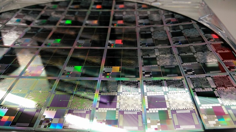
Recent research demonstrates the transformative potential: Early High-NA results show successful patterning of 8-nanometer line widths—dimensions that were previously impossible with any lithography technique. For comparison, these features are roughly 10 times smaller than the smallest virus and 1,000 times thinner than a human hair. At this scale, 2nm transistors can achieve densities exceeding 300 million transistors per square millimeter.
The numerical aperture improvement enables more than just smaller features—it fundamentally changes manufacturing economics. Traditional multiple-patterning techniques required for current EUV systems add 3-5 additional processing steps per layer, increasing costs by $50-100 per wafer. High-NA EUV can pattern the same features in single exposures, dramatically reducing manufacturing complexity and cost.
The $350+ Million Engineering Marvel: Building Tomorrow’s Manufacturing Tools
Behind High-NA EUV’s breakthrough capabilities lies perhaps the most complex manufacturing machine ever created. Each ASML EXE:5000 High-NA system represents one of the most expensive and complex manufacturing machines ever created, with costs exceeding $350 million per unit. These aren’t just expensive tools—they represent the absolute pinnacle of precision engineering, combining technologies from quantum physics, materials science, and advanced robotics.
The core challenge lies in creating and controlling extreme ultraviolet light. Unlike visible light, EUV wavelengths are absorbed by virtually all materials, requiring complete vacuum operation and specialized mirror coatings. The EUV source itself generates plasma temperatures exceeding 200,000°C—nearly 20 times hotter than the Sun’s surface—by firing high-powered lasers at molten tin droplets just 30 micrometers in diameter.
Each tin droplet must be precisely positioned in three dimensions to within 2 micrometers, while traveling at 70 meters per second. The timing precision required surpasses that of Formula 1 race cars: missing the target by even microseconds ruins the exposure. When successful, this process generates approximately 250 watts of usable EUV power—enough to illuminate a large room if it were visible light.
The optical system presents even greater challenges. High-NA systems employ six ultra-precise mirrors, each polished to tolerances measured in fractions of atoms. Creating mirrors with 0.55 numerical aperture requires aspherical shapes so complex that manufacturing a single mirror takes 18 months of continuous polishing and measuring cycles.
The environmental controls border on science fiction: The entire system operates in ultra-high vacuum (10^-9 torr), requiring contamination levels 100 billion times lower than atmospheric pressure. Think of it as creating a cleaner environment inside this machine than exists in outer space—because even a single water molecule can contaminate the delicate EUV optics.
Vibration isolation systems cancel building movements, passing trucks, and even distant earthquakes. Temperature control maintains stability to within 0.001°C across the entire massive machine. It’s like maintaining the temperature of an Olympic swimming pool to within the warmth of a single breath—while the pool is the size of a building and weighs as much as a jumbo jet.
Manufacturing throughput demands add another layer of complexity. Each High-NA system must process 120-150 wafers per hour to be economically viable—that’s one complete wafer every 25-30 seconds. Achieving this pace requires robotic wafer handling systems with acceleration tolerances measured in micro-g’s to prevent mechanical damage to delicate silicon substrates.
Intel’s investment reveals the manufacturing reality: Their first High-NA system, delivered in December 2023, represents just the beginning of a planned major manufacturing expansion. Intel expects to operate multiple High-NA systems by the late 2020s, enabling production of advanced AI processors with transistor features that were physically impossible to manufacture just two years ago.
The economic implications extend beyond manufacturing costs. High-NA EUV enables “single-patterning” techniques that reduce 2nm manufacturing to 15-20 processing steps instead of the 50+ steps required with current multi-patterning approaches. This simplification could reduce 2nm chip production costs by 30-40% compared to alternative approaches, making advanced AI processors economically viable for broader markets.
The 2nm Reality Check: Where Physics Meets Manufacturing Precision
While High-NA EUV solves the fundamental resolution limitations, creating viable 2nm transistors requires conquering a cascade of additional physics and engineering challenges. At 2nm dimensions, individual atoms matter: a single misplaced silicon atom can alter transistor behavior, and contamination particles smaller than viruses can destroy entire chips.
The manufacturing precision requirements stretch beyond current capabilities. 2nm transistors require gate oxide layers just 1-2 atoms thick, with thickness variations controlled to 0.1 angstrom—roughly 1/100th the diameter of a hydrogen atom. Traditional silicon dioxide gate oxides become unstable at these dimensions, requiring exotic high-k dielectric materials like hafnium oxide with precisely controlled crystalline structure. For perspective, achieving this precision is like building a house with walls exactly two playing cards thick, where being off by the thickness of a single atom would cause the entire structure to fail.
Metal deposition presents equally daunting challenges: Interconnect wires must be patterned to widths below 15 nanometers while maintaining electrical resistance low enough for high-speed operation. At these dimensions, surface scattering effects dominate electrical behavior, requiring specialized copper alloys and barrier materials with atomic-level optimization. This is electrical engineering at the molecular scale—where individual atoms of impurities can block electrical current like boulders blocking a narrow stream.
Heat dissipation becomes critical at 2nm scales. Transistor switching generates localized heating that, at sub-10nm dimensions, can exceed 1,000°C for nanosecond intervals. Managing these thermal spikes requires new gate materials with thermal conductivities 10 times higher than traditional options, pushing materials science into uncharted territory.
Current manufacturing results reveal both progress and remaining challenges. Early 2nm prototypes from leading manufacturers demonstrate transistor densities approaching 300 million per square millimeter, with potential performance improvements of 40-50% over current 3nm designs. However, manufacturing yields for these advanced processes remain challenging, with industry reports suggesting initial yields significantly below mature technology nodes.
TSMC’s approach emphasizes manufacturing optimization over speed-to-market: Their 2nm roadmap prioritizes yield improvement and cost reduction, potentially achieving 60-70% manufacturing yields by 2027. This yield advantage could translate to 2-3x cost advantages over competitors, determining market leadership in advanced processor manufacturing.
The timeline reality reflects these challenges. While High-NA EUV systems enable 2nm patterning today, achieving volume manufacturing requires 18-24 months of process optimization per new technology node. Intel’s 2nm production timeline targets late 2024 for initial production, with volume manufacturing beginning in 2025—assuming current optimization rates continue.
For AI processor applications, 2nm technology promises transformational capabilities: 50% higher performance combined with 30% lower power consumption enables AI training systems with 3x computational efficiency. Mobile AI processors could achieve desktop-class performance while maintaining all-day battery life. These improvements aren’t incremental—they represent the performance leaps necessary to enable next-generation AI applications from autonomous vehicles to real-time language translation.
The competitive implications extend beyond individual companies. Nations view advanced semiconductor manufacturing as critical infrastructure, leading to massive government investments: The U.S. CHIPS Act allocates $52 billion for domestic semiconductor production, while the European Chips Act targets €43 billion for advanced manufacturing capabilities. High-NA EUV systems represent the core technology enabling these strategic manufacturing goals.
References
[1] Semiconductor Engineering, “High-NA EUV Lithography,” 2024.
[2] SPIE Proceedings, “High numerical aperture extreme ultraviolet lithography for 2 nm and beyond,” 2019.
[3] IEEE Spectrum, “The Semiconductor Industry’s Most Important Tool Goes Green,” 2024.
[4] SemiWiki, “High-NA EUV Lithography Roadmap,” 2024.
[5] Nature Physics, “Extreme ultraviolet lithography: Physics of photoresist materials,” 2015.
[6] Applied Physics Reviews, “Critical challenges in high numerical aperture extreme ultraviolet lithography,” 2021.
[7] Physics World, “High-NA EUV lithography takes shape,” 2023.
[8] OSA Optics Express, “Numerical aperture scaling in EUV lithography systems,” 2020.
This digest was generated by AaBot using real-time web and literature research.