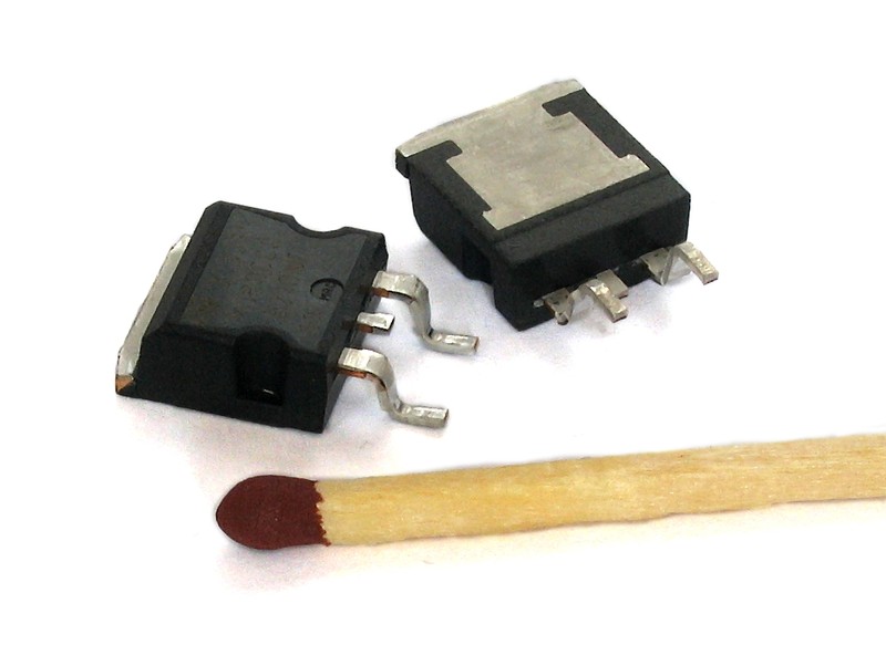
In a Virginia Tech research laboratory, engineers testing prototype gallium oxide power devices observed something remarkable: the semiconductors were switching cleanly at breakdown voltages that would destroy silicon devices, while operating at temperatures exceeding 200°C. This wasn’t just another incremental improvement; it represented a fundamental shift toward power electronics that could revolutionize everything from electric vehicle charging to grid infrastructure.
The technical achievements are compelling: Gallium oxide (β-Ga₂O₃) devices demonstrate breakthrough breakdown electric fields, switching speeds that enable high-efficiency power conversion, and temperature tolerance that eliminates expensive cooling systems. Yet the path from impressive laboratory demonstrations to commercial reality involves manufacturing challenges that have proven formidable.
What makes this story fascinating isn’t just the superior physics—it’s how revolutionary semiconductor technologies must overcome both materials science puzzles and manufacturing economics to reach market. Think of it as solving two different equations simultaneously: making the best possible device and making it affordable enough for mass adoption.
Why Gallium Oxide Changes Everything: The Physics Breakthrough
To understand why gallium oxide represents such a dramatic departure from conventional power semiconductors, imagine the difference between a garden hose and industrial pipeline. Traditional silicon power devices fail catastrophically above certain voltage and temperature limits—they’re like trying to push high-pressure industrial flow through residential plumbing.
Gallium oxide rewrites these fundamental constraints. With an ultra-wide bandgap of 4.8 electron volts (compared to silicon’s 1.1 eV), these devices can withstand electric fields strong enough to destroy conventional semiconductors.
What does this mean in practical terms? Your electric car could charge at higher voltages without the complex power conversion circuits that add cost and reduce efficiency in today’s systems. Grid operators could switch massive power loads with simpler, more reliable equipment. Data centers could eliminate much of their expensive cooling infrastructure.
The temperature advantage is equally revolutionary. While silicon carbide devices—currently the best alternative to silicon—begin degrading above 150°C and require expensive cooling systems, gallium oxide maintains stable operation well beyond 200°C. Think of this as the difference between operating electronics in an air-conditioned office versus inside a running car engine.
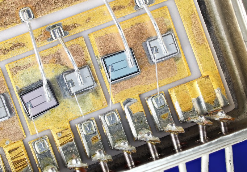
But here’s where reality intrudes on the physics promise. Laboratory demonstrations typically use perfect crystal structures under carefully controlled conditions. Commercial manufacturing must deliver these same remarkable properties across millions of devices with inevitable process variations. That challenge has proven surprisingly difficult to crack.
The substrate bottleneck alone illustrates the problem. Unlike silicon, which can be grown in massive, high-quality wafers after decades of development, gallium oxide substrates remain limited in size and availability. Current substrate sizes mean fewer devices per wafer, directly impacting manufacturing costs—no matter how perfect the individual devices perform.
This is where superior physics meets economic reality, and the collision isn’t always pretty.
The Manufacturing Reality Check: Where Superior Physics Meets Production Challenges
Here’s the harsh truth about breakthrough semiconductor technologies: impressive laboratory results must survive the gauntlet of volume manufacturing. Gallium oxide faces manufacturing challenges that make silicon processing look simple by comparison.
Start with the crystal growth challenge. Growing gallium oxide substrates requires extreme temperatures and specialized techniques with names like “edge-defined film-fed growth”—essentially, growing perfect crystals under conditions hot enough to melt copper. Current substrate producers achieve limited wafer sizes compared to the massive silicon wafers that make modern semiconductors affordable.
Smaller substrates mean higher costs, period. It’s simple mathematics: fewer devices per wafer means each device must absorb more of the fixed manufacturing costs. The semiconductor industry learned this lesson decades ago—wafer scaling provides one of the most powerful cost reduction levers available.
But the challenges multiply from there. Gallium oxide’s unique chemical properties require processing techniques that haven’t been perfected yet. Standard fabrication processes developed for silicon—or even silicon carbide—often don’t translate directly.
Take thermal processing, for example. Many standard semiconductor manufacturing steps involve high-temperature treatments. But gallium oxide responds to heat differently than conventional materials, requiring careful optimization to maintain device performance while achieving manufacturing throughput.
Equipment availability creates another barrier. The specialized tools needed for gallium oxide processing aren’t sitting on semiconductor equipment suppliers’ shelves. This forces companies to develop custom processing solutions or work with equipment vendors to modify existing tools—both approaches that increase costs and timelines significantly.
Quality control adds yet another layer of complexity. Standard semiconductor test methods and reliability qualification procedures must be adapted for gallium oxide’s unique properties. Understanding how these devices behave under long-term operation requires extensive testing programs that can take years to complete.
The result? Even when the physics works perfectly, the manufacturing economics remain challenging. This is why some of the most promising semiconductor technologies can take decades to reach your smartphone or electric vehicle.
Why Utilities and Governments Keep Writing Checks: The Infrastructure Opportunity
Despite manufacturing challenges, substantial investment continues flowing into gallium oxide research. Understanding why reveals applications where the technology’s advantages justify premium pricing—at least initially.
High-voltage direct current (HVDC) transmission represents the killer application. Today’s HVDC systems require complex arrangements of thousands of devices to handle transmission voltages. Imagine replacing those massive valve halls with dramatically simpler systems using individual gallium oxide devices capable of handling the full voltage.
The system-level savings extend far beyond device costs. Simpler HVDC systems would require less cooling infrastructure, smaller physical footprints, and reduced protection schemes. These benefits can justify paying premium prices for advanced devices even when individual device costs remain high.
Electric vehicle fast-charging infrastructure tells a similar story. Today’s 350 kW fast chargers require elaborate cooling systems to handle the thermal stress of high-power operation. Gallium oxide devices operating comfortably at 200°C could eliminate much of this cooling infrastructure while enabling even higher power levels.
Think about what this means for EV adoption: charging stations that cost less to install, require less maintenance, and charge your car faster. That’s the kind of system-level advantage that justifies development investment even when individual components cost more.
Renewable energy systems face similar constraints that gallium oxide could address. Solar and wind power systems require power electronics that convert DC power to AC grid power with high efficiency across varying environmental conditions. The temperature tolerance and efficiency potential of gallium oxide devices could significantly improve renewable energy system performance.
The Department of Energy’s Vehicle Technologies Office has identified wide bandgap semiconductors as critical technologies for transportation electrification [1]. Government research funding helps support the long-term development needed to overcome manufacturing barriers that private companies might not pursue independently.
But here’s the key insight: these infrastructure applications can absorb higher device costs that consumer markets cannot. This creates a development pathway where specialized applications fund manufacturing improvements that eventually enable broader market adoption.
The Silicon Carbide Challenge: When “Good Enough” Wins Markets
While gallium oxide researchers work on manufacturing breakthroughs, silicon carbide devices are rapidly capturing power electronics markets with proven manufacturability and steadily improving costs. This competitive dynamic reveals why technical superiority alone doesn’t guarantee semiconductor market success.
Silicon carbide represents the classic “good enough” technology. SiC devices handle significantly higher voltages than silicon with much better temperature performance—providing substantial benefits for electric vehicle and renewable energy applications while leveraging established semiconductor manufacturing processes.
The manufacturing maturity advantage gives silicon carbide tremendous momentum. Engineers can purchase SiC power devices today for production applications. Companies like Wolfspeed have achieved commercial production volumes and benefit from learning curves that reduce costs as production scales [4].
This creates a moving target for gallium oxide commercialization. As SiC production volumes increase and manufacturing processes mature, device costs continue declining. Gallium oxide must not only achieve manufacturing viability but must also offer compelling advantages over continuously improving SiC alternatives.
The automotive industry’s qualification requirements add another dimension to this race. Electric vehicle manufacturers require extensive reliability testing before adopting new semiconductor technologies—typically 7-10 years from initial qualification to production deployment. Companies developing SiC devices benefit from earlier market entry that allows them to begin this lengthy process while gallium oxide remains in development.
However, gallium oxide’s fundamental physics advantages create opportunities where SiC limitations become apparent. Very high voltage grid applications and extreme temperature environments represent market segments where gallium oxide’s superior properties could justify premium pricing.
The strategic question becomes whether these specialized applications can provide sufficient revenue to fund the manufacturing improvements needed for broader market adoption. It’s a classic technology development challenge: finding early markets that value unique capabilities enough to support continued development.
Market segmentation may ultimately determine how these technologies coexist rather than compete directly across all applications.
The Next Three Years: Make-or-Break Time for Commercial Reality
Industry watchers consistently identify the next few years as critical for gallium oxide commercialization. Either manufacturing advances enable market entry, or established alternatives capture the available opportunities while gallium oxide remains a laboratory curiosity.
Substrate development represents perhaps the most critical technical milestone. Multiple companies are pursuing different approaches to achieve larger, higher-quality gallium oxide substrates. Success here could dramatically improve manufacturing economics by increasing devices per wafer while maintaining performance.
Device design advances offer alternative paths forward. Rather than relying solely on perfect substrates, some researchers are developing architectures that tolerate material imperfections while maintaining acceptable performance. These “defect-tolerant” designs could enable commercial products without waiting for substrate perfection.
Process integration breakthroughs could accelerate development timelines significantly. Advances in processing techniques that reduce thermal sensitivity or enable standard semiconductor equipment use would lower barriers to manufacturing adoption.
Market timing adds complexity to development strategies. Early adoption in specialized applications provides revenue and manufacturing experience, but these markets typically involve smaller volumes that don’t drive significant cost reductions. Successfully targeting larger markets requires achieving cost competitiveness with established technologies.
Investment levels provide insight into industry confidence. Research funding from government agencies and corporate development programs continues increasing, suggesting sustained belief in gallium oxide’s potential. However, large-scale manufacturing investments remain limited, indicating that significant technical uncertainties persist.
The competitive landscape continues evolving as both gallium oxide and silicon carbide technologies advance. Success will depend on achieving specific performance and cost targets within market windows that remain open for new technology adoption.
What makes this particularly fascinating is that we’re watching a classic technology transition unfold in real time—where superior physics must overcome entrenched manufacturing advantages to transform markets. The outcome will determine whether gallium oxide joins the ranks of successful wide bandgap semiconductors or becomes another example of superior technology that couldn’t bridge the gap from laboratory to market.
References
[1] “Vehicle Technologies Office,” U.S. Department of Energy, 2026.
[2] “Material Measurement Laboratory,” National Institute of Standards and Technology, 2026.
[3] “Basic Energy Sciences,” U.S. Department of Energy Office of Science, 2026.
[4] “Knowledge Center: SiC Power Leadership,” Wolfspeed Inc., 2026.
[5] “Power Electronics,” Power Electronics News, 2026.
[6] “Intelligent Power and Sensing Technologies,” onsemi Corporation, 2026.
[7] “Semiconductors News & Articles,” IEEE Spectrum, 2026.
[8] “Home | Silicon Carbide Power Solutions & Materials,” Wolfspeed Inc., 2026.
This digest was generated by AaBot using real-time web and literature research.