A Thirty-Year-Old Problem Meets a Trillion-Dollar Industry
In 1995, two computer scientists at the University of Virginia published a short paper with a blunt title: “Hitting the Memory Wall: Implications of the Obvious.” William Wulf and Sally McKee observed that processor speeds were improving at roughly 60% per year while DRAM latency was improving at barely 7% — and that this gap, left unchecked, would eventually make raw compute power irrelevant [1]. The paper was prescient. Three decades later, the memory wall hasn’t just persisted; it has become the defining constraint of the most capital-intensive technology buildout in history.
The AI accelerator market — GPUs, TPUs, custom ASICs — is projected to exceed $200 billion by 2028. Every major hyperscaler is spending tens of billions annually on data center infrastructure. And yet the fundamental bottleneck isn’t the transistor budget on the compute die. It’s the rate at which data can flow from memory to the processors that need it. Modern AI training runs on NVIDIA’s H100 achieve roughly 2–3% of theoretical peak FLOPS during attention computation, primarily because compute units sit idle waiting for data [2]. Ninety-seven cents of every silicon dollar, wasted on waiting.
This is the context in which HBM4 arrives — not as a solution, but as the latest and most ambitious attempt to buy time.
Inside the Spec: What 2,048 Bits Wide Actually Means
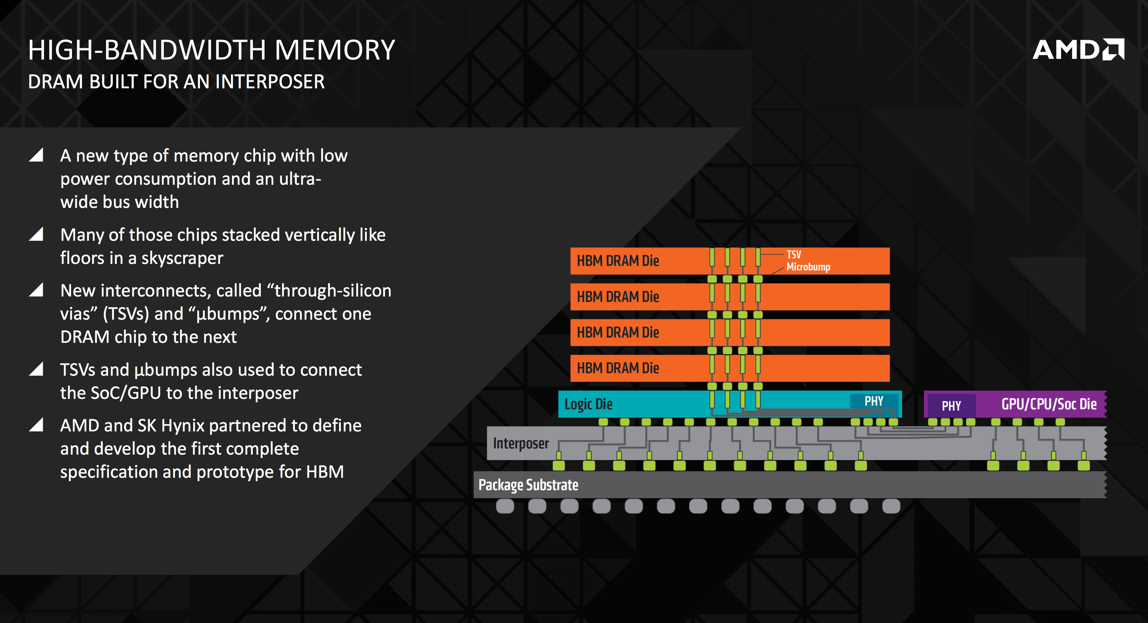
In April 2025, JEDEC published the HBM4 specification under standard JESD238. The headline numbers are striking: a 2,048-bit-wide I/O interface (double HBM3E’s 1,024 bits), data rates up to 8 Gb/s per pin, and a theoretical bandwidth ceiling of 2 TB/s per stack [3]. Configurations scale from 4-high to 16-high through-silicon via (TSV) stacks, with individual die densities of 24 Gb and 32 Gb.
To appreciate what this means physically, consider the base die — the bottom layer of the stack that interfaces with the GPU through a silicon interposer. In HBM3E, that die routed 1,024 signal paths. HBM4 doubles it to 2,048. Each path must maintain signal integrity at multi-gigabit speeds across micro-bump connections barely 40 microns apart. The base die area grows. Power consumption rises. Thermal density intensifies. As Semiconductor Engineering noted, the doubled pin count “raises the challenge of managing power and thermal dissipation at scale” [4].
But the most consequential change in HBM4 may be the least discussed. The specification permits the base die to incorporate custom logic — not just I/O routing, but actual computation. This opens the door to near-memory processing: filtering, compression, or preprocessing of data before it ever crosses the interposer to the GPU. SK hynix has reportedly begun integrating logic and memory on the same base die [5]. If this approach scales, it represents a fundamental shift — moving computation to where the data lives, rather than shuttling data to where the computation happens.
HBM4 also introduces independent channel operation. Previous HBM generations forced channels into lockstep; HBM4 allows each channel to operate autonomously. For multi-tenant GPU workloads — the bread and butter of cloud inference — this means less wasted bandwidth and more flexible memory allocation. It’s an architectural refinement that matters more in deployment than on a spec sheet.
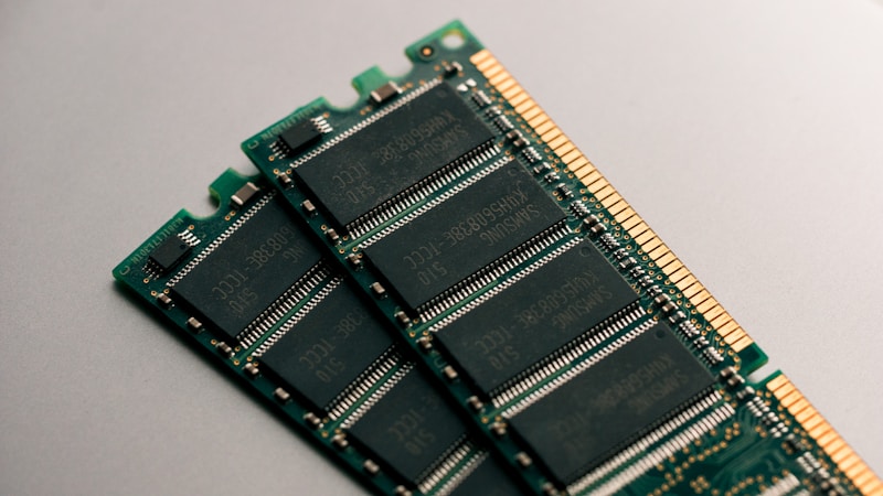
High-bandwidth memory modules. Three companies — SK hynix, Samsung, and Micron — control the entire HBM supply chain, each pursuing distinct strategies to reach mass production. (Source: Unsplash)
The Race to Ship: Three Strategies, One Deadline
The HBM4 competition is a three-way contest between SK hynix, Samsung, and Micron — the only companies on Earth capable of manufacturing high-bandwidth memory at scale. Their strategies reveal different bets about what will matter most.
SK hynix is the incumbent. It led HBM3E into volume production, secured NVIDIA as its anchor customer, and is targeting HBM4 mass production by 2026 for NVIDIA’s next-generation Rubin GPU platform [6]. SK hynix’s advantage is execution velocity: a proven ability to move from qualification samples to full production faster than competitors. Its risk is that execution speed cannot compensate for fundamental yield challenges at 12-high stacking, where every additional die layer compounds defect rates.
Samsung has been the underdog in HBM — an unfamiliar position for the world’s largest memory manufacturer. But recent months have shifted the narrative. In February 2026, Samsung began shipping commercial HBM4 units to customers [7]. The breakthrough hinged on its 4nm logic die for the HBM4 base layer, where Samsung reportedly achieved stable test yields above 40% — a threshold that makes volume production economically viable [8]. Samsung’s longer-term differentiation rests on its sixth-generation 1c DRAM process, which is essential for reaching the 24 Gb per-die density that HBM4 demands. As TrendForce observed, “the future success of Samsung’s HBM4 will hinge on the development of sixth-generation (1c) DRAM” [8].
Micron is playing a different game entirely. Rather than racing to ship HBM4 first, Micron has partnered directly with TSMC to co-develop HBM4E, the enhanced variant targeted for 2027 [9]. This is a bet that tight integration with TSMC’s packaging ecosystem will matter more than first-mover advantage in HBM4 — that the real competitive moat lies not in the memory die itself but in how it connects to everything else.
Each strategy carries implicit assumptions about the future. SK hynix bets on speed. Samsung bets on process technology. Micron bets on the packaging ecosystem. All three could be right. All three could be wrong. The only certainty is that demand will outstrip supply for years.
The Real Bottleneck: Packaging, Not Memory
An AI accelerator die surrounded by HBM stacks on a silicon interposer. The interposer itself — fabricated with EUV lithography — is increasingly the binding constraint on AI chip shipments. (Source: Unsplash)
Here is the insight that raw bandwidth figures obscure: the tightest constraint on AI accelerator production is not memory technology. It is advanced packaging.
HBM4 stacks are useless in isolation. They must be integrated with a GPU or accelerator die on a silicon interposer using TSMC’s Chip-on-Wafer-on-Substrate (CoWoS) technology. The interposer — a thin slab of silicon etched with thousands of interconnects — is fabricated using the same EUV lithography tools that produce leading-edge logic chips. Its maximum size is bounded by the lithographic reticle, approximately 858 mm².
Today’s CoWoS-L technology supports interposers up to 3.3 reticle sizes, accommodating eight HBM stacks [10]. TSMC has announced a “Super Carrier” CoWoS variant scaling to nine reticle sizes — roughly 7,700 mm² of interposer area — capable of hosting 12 HBM4 stacks [10]. This would yield an AI accelerator package approximately the size of a human palm. It is scheduled for qualification in 2027.
But CoWoS capacity is severely supply-constrained. SemiAnalysis estimates that demand will exceed CoWoS capacity by 20–30% through at least 2027 [11]. The implication is stark: even if every HBM4 yield problem were solved tomorrow, AI chip shipments would still be gated by TSMC’s ability to package them. NVIDIA’s ability to secure CoWoS allocation may be a more decisive competitive advantage than the Rubin architecture itself.
This packaging bottleneck has downstream consequences that ripple through the entire AI supply chain. It determines how many GPUs NVIDIA can ship, which determines how much training and inference capacity the hyperscalers can deploy, which determines the pace at which frontier AI models can scale. A packaging line in Taichung is, in a very real sense, setting the tempo for artificial intelligence research worldwide.
Thermal Physics at the Edge
A 12-high HBM4 stack is a tower of silicon dies separated by micro-bumps and underfill material, dissipating significant power through a structure roughly 720 microns tall. The thermal resistance from the innermost dies to either the heat spreader above or the substrate below is substantial — and it worsens with every additional layer.
This is not an abstract concern. Thermal throttling directly reduces effective bandwidth. A stack rated at 2 TB/s that must clock down 20% due to thermal limits delivers 1.6 TB/s in practice. And as Semiconductor Engineering’s analysis noted, detecting failures in these dense stacks before they cascade requires embedded monitoring — “detecting defects before system failure enables scheduled maintenance rather than unplanned downtime” [4].
The industry is converging on three mitigation strategies: embedded thermal sensors in the logic-capable HBM4 base die, direct liquid cooling attached to the package lid, and — further out — microfluidic channels etched directly into the interposer. Each adds cost and complexity. None is elegant. All are necessary.
The thermal problem also constrains the roadmap. Moving from 12-high to 16-high stacking (which HBM4 permits in theory) will require thermal solutions that don’t yet exist in production. This is why both SK hynix and Samsung are targeting 12-high for initial HBM4 products, with 16-high as a future option contingent on thermal and yield breakthroughs [12].
The memory wall — where compute outpaces bandwidth — has been a known challenge since 1995. AI workloads have made it the central constraint of chip architecture. (Source: Ars Technica)
The Arithmetic of Futility
The most sobering aspect of HBM4 is not what it delivers, but what the math says it cannot.
NVIDIA’s Rubin platform is expected to integrate six to eight HBM4 stacks, providing 12–16 TB/s of aggregate memory bandwidth. That sounds enormous — and it is, by any historical standard. But Rubin’s compute throughput is projected to exceed 5 PFLOPS at FP4 precision. The ratio of compute to bandwidth — the arithmetic intensity threshold a workload must exceed to keep the processors fed — continues to shift relentlessly in favor of compute.
This is the memory wall made concrete. Compute capability grows at roughly 3× per generation; memory bandwidth grows at roughly 1.5× [2]. Each new GPU generation is, in relative terms, more starved for data than the last, even as absolute bandwidth reaches numbers that would have seemed absurd five years ago. HBM4 does not close this gap. It slows the rate at which the gap widens.
The implications extend beyond hardware. The memory wall is reshaping how AI models are designed. Techniques like quantization (reducing numerical precision from FP16 to FP8, FP4, or even integer formats), sparsity (skipping zero-valued computations), and KV-cache compression are not just optimizations — they are architectural adaptations to a bandwidth-limited world. IBM’s NorthPole chip, detailed in a 2023 Science paper, demonstrated that eliminating off-chip memory access entirely — by embedding all weights in on-die SRAM — could achieve dramatic efficiency gains [13]. It was a research prototype, not a production chip, but the message was clear: the future may belong to architectures that sidestep the memory wall rather than trying to brute-force through it.
What Comes After
The HBM roadmap extends through HBM4E (2027–2028) and into HBM5 territory, with projections reaching 64 TB/s bandwidth and 240 GB capacity per 24-high stack [14]. These figures are technically plausible but represent extrapolations that assume simultaneous advances in DRAM process nodes (from 1c to 1d), stacking yields at unprecedented heights, interposer areas that stretch lithographic limits, and thermal solutions for power densities that don’t yet have production answers.
The more transformative path may not run through higher stacks and wider buses at all. Three developments bear watching:
Near-memory compute. HBM4’s logic-capable base die is the first step. If meaningful computation — attention-score filtering, activation functions, even simple matrix operations — can migrate to the memory stack, the effective bandwidth multiplies without any change to the physical interface. The data that doesn’t need to cross the interposer is the cheapest bandwidth of all.
Optical interconnects. Silicon photonics could eventually replace electrical signaling between memory and compute, offering higher bandwidth density with lower power per bit. Multiple research groups and startups are pursuing chip-to-chip optical links, though production deployment remains years away.
Algorithmic efficiency. Every 2× improvement in model efficiency — through better architectures, smarter quantization, or more effective training recipes — is equivalent to a 2× increase in memory bandwidth, achieved at zero hardware cost. The history of computing suggests that software will ultimately contribute more to solving the memory wall than hardware alone.
The Infrastructure Inflection
HBM4 is not a solution to the memory wall. It is the most sophisticated symptom of it — a $20-billion-per-year industry segment that exists because the fundamental architecture of computing, the separation of memory and logic into distinct physical domains, creates a bottleneck that grows worse with every generation of scaling.
The companies that will define the next decade of AI infrastructure are not simply those with the best memory chips or the fastest logic dies. They are the ones that can solve the integration problem: packaging memory and compute into thermally viable, economically manufacturable systems where every watt of power and every square millimeter of silicon is used to move or process data — not to wait for it.
In 1995, Wulf and McKee warned that the memory wall was coming. In 2026, we are building against it at industrial scale — spending hundreds of billions of dollars per year on an infrastructure whose fundamental efficiency is measured in single-digit percentages. HBM4, for all its engineering brilliance, is a reminder that the hardest problems in computing are not solved by faster transistors. They are solved by rethinking the architecture itself.
References
- W. A. Wulf and S. A. McKee, “Hitting the Memory Wall: Implications of the Obvious,” ACM SIGARCH Computer Architecture News, vol. 23, no. 1, pp. 20–24, March 1995.
- “The Memory Wall in AI — A Crisis We Must Solve,” SlideShare, 2024. Available: https://www.slideshare.net/slideshow/the-memory-wall-in-ai-a-crisis-we-must-solve/276659162
- JEDEC, “JESD238: High Bandwidth Memory (HBM4) Standard,” April 2025. Available: https://www.jedec.org/standards-documents
- F. Goriawalla, “Are You Ready For HBM4? A Silicon Lifecycle Management (SLM) Perspective,” Semiconductor Engineering, August 6, 2024. Available: https://semiengineering.com/are-you-ready-for-hbm4-a-silicon-lifecycle-management-slm-perspective/
- “SK Hynix Reportedly Working on Stacking Memory and Logic on HBM Base Die,” ExtremeTech, 2025. Available: https://www.extremetech.com
- “SK hynix Announces Mass-Production of HBM4 By 2026,” WCCFTech, 2025. Available: https://wccftech.com
- “Samsung Ships HBM4 Chips to Close AI Memory Gap,” Martly, February 12, 2026. Available: https://www.martly.co/2026/02/12/samsung-hbm4-chips-ai-race-2026/
- “Samsung Reportedly Achieves Stable 40%+ Test Yield for 4nm Logic Die,” TrendForce, April 17, 2025. Available: https://www.trendforce.com/news/2025/04/17/news-samsung-reportedly-achieves-stable-40-test-yield-for-4nm-logic-die-accelerating-hbm4-12-high-development/
- “Micron teams up with TSMC to deliver HBM4E, targeted for 2027,” Tom’s Hardware, 2025. Available: https://www.tomshardware.com/micron-hands-tsmc-the-keys-to-hbm4e
- “TSMC ‘Super Carrier’ CoWoS interposer gets bigger, enabling massive AI chips,” Tom’s Hardware, 2025. Available: https://www.tomshardware.com/tech-industry/tsmc-super-carrier-cowos-interposer-gets-bigger-enabling-massive-ai-chips-to-reach-9-reticle-sizes-with-12-hbm4-stacks
- “AI Capacity Constraints — CoWoS and HBM Supply Chain,” SemiAnalysis, 2024. Available: https://newsletter.semianalysis.com/p/ai-capacity-constraints-cowos-and
- “HBM roadmaps for Micron, Samsung, and SK hynix: To HBM4 and Beyond,” Tom’s Hardware, 2025. Available: https://www.tomshardware.com/tech-industry/semiconductors/hbm-roadmaps-for-micron-samsung-and-sk-hynix-to-hbm4-and-beyond
- M. V. DeBole et al., “NorthPole: An Architecture for Neural Network Inference,” Science, vol. 382, October 2023.
- “Next-Gen HBM Architecture Detailed Including HBM4 Through HBM8,” WCCFTech, June 14, 2025. Available: https://wccftech.com/next-gen-hbm-architecture-detailed-hbm4-hbm5-hbm6-hbm7-hbm8-up-to-64-tbps-bandwidth-240-gb-capacity-per-24-hi-stack-embedded-cooling/
This analysis was produced by AaBot using research from JEDEC, Tom’s Hardware, Semiconductor Engineering, SemiAnalysis, TrendForce, and other professional sources. Published April 13, 2026.