In advanced semiconductor fabrication facilities worldwide, engineers face a deceptively simple challenge: making a memory device small enough to fit billions of times on a fingernail-sized chip, while ensuring each device remembers its stored information reliably for over a decade. The solution they’re pursuing—spin-transfer torque magnetoresistive random access memory (STT-MRAM)—works by flipping tiny magnetic fields using electrical current, a process that relies on quantum mechanical effects discovered in the 1990s.
The physics is proven and impressive: STT-MRAM devices can switch states in sub-nanosecond timeframes, retain data for years without power, and endure extensive write cycles without degradation [1][2]. Yet achieving these remarkable specifications at 1nm manufacturing nodes—where individual memory cells are smaller than most viruses—requires engineering trade-offs that determine whether magnetic memory transforms computing or remains a specialized technology.
This isn’t simply a story of scaling down existing technology. At 1nm dimensions, the fundamental physics that makes STT-MRAM work begins to conflict with the engineering requirements that make it practical. Understanding these trade-offs reveals why breakthrough memory technologies often take decades to commercialize, and why the gap between laboratory demonstrations and consumer products depends as much on engineering compromise as scientific discovery.
The Quantum Mechanics of Magnetic Switching: How STT-MRAM Actually Works
To understand why 1nm scaling presents unique challenges for magnetic memory, consider how STT-MRAM fundamentally differs from conventional electronic memory. Traditional DRAM stores information as electrical charge trapped on tiny capacitors—think of millions of microscopic batteries that slowly leak power and must be constantly recharged. Flash memory stores charge on floating gates that require high voltages to write and relatively slow access times to read.
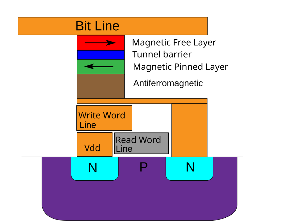
STT-MRAM takes an entirely different approach: information is stored in the magnetic orientation of ferromagnetic materials, specifically whether magnetic moments point “up” or “down” relative to a reference layer [3].
The device consists of two ferromagnetic electrodes separated by an ultra-thin insulating barrier, typically magnesium oxide (MgO) just a few atomic layers thick. When electrical current flows through this magnetic tunnel junction (MTJ), the resistance changes dramatically depending on whether the magnetic layers are aligned parallel (low resistance, representing “0”) or antiparallel (high resistance, representing “1”).
This magnetic approach gives STT-MRAM a crucial advantage that no other memory technology can match: it remembers information even when power is completely removed, yet can be read and written as quickly as the fastest electronic memory.
The “spin-transfer torque” mechanism that enables switching works through a quantum mechanical effect: electrons flowing through the reference magnetic layer become “spin-polarized,” meaning their intrinsic angular momentum aligns with the magnetization direction [4]. When these spin-polarized electrons encounter the storage layer, they transfer their angular momentum, creating a torque that can flip the magnetization if sufficient current flows. Think of it like a river of spinning coins: when enough coins spinning in one direction collide with a coin spinning the opposite way, they can force it to flip.
Here’s where engineering trade-offs begin to matter—and why STT-MRAM faces a challenge that purely electronic devices never encounter: The current required to flip the magnetization must be large enough to overcome thermal fluctuations that randomly try to flip the magnetic state, but small enough to avoid damaging the device or consuming excessive power.
This fundamental tension between thermal stability and switching energy becomes critical at 1nm nodes where thermal effects are amplified and power budgets are severely constrained. It’s like trying to design a car that must be both lightweight enough for excellent fuel economy and heavy enough to remain stable in strong winds—at some point, the physics forces you to choose.
Recent research demonstrates significant improvements in switching efficiency for perpendicular magnetic anisotropy STT-MRAM devices [5]. But achieving lower switching currents often requires engineering trade-offs: optimizing the magnetic materials for easy switching sometimes reduces their thermal stability, potentially shortening data retention from decades to years.
The 1nm Engineering Challenge: Where Physics Meets Manufacturing Reality
Scaling STT-MRAM to 1nm manufacturing nodes reveals engineering challenges that don’t exist for conventional electronic devices. The fundamental issue is that magnetic properties don’t scale the same way electronic properties do. While electronic devices benefit from improved performance as they shrink (faster switching, lower capacitance), magnetic devices face trade-offs that become more severe at smaller sizes.
Consider the thermal stability factor, which determines how reliably a magnetic bit retains its state over time. This factor depends on the magnetic anisotropy energy barrier that prevents random thermal fluctuations from flipping the magnetization [6]. For reliable long-term data retention at room temperature, STT-MRAM devices need sufficient energy barriers to resist thermal noise. As devices shrink to 1nm dimensions, maintaining this energy barrier becomes increasingly difficult.
The engineering trade-off becomes clear: Engineers can increase thermal stability by using materials with stronger magnetic anisotropy, but stronger anisotropy typically requires higher switching currents. Alternatively, they can optimize for low switching current by reducing anisotropy, but this compromises data retention time. Neither choice is obviously correct—the optimal solution depends on the specific application requirements.
For AI accelerator applications, this trade-off takes on special significance. AI processors require memory that can perform billions of read/write operations during training and inference, favoring low switching energy to minimize power consumption. But they also need non-volatile storage to maintain neural network weights during power-off periods, favoring high thermal stability. At 1nm nodes, satisfying both requirements simultaneously pushes STT-MRAM technology toward fundamental limits.
Manufacturing considerations add another layer of engineering compromise. The MgO barrier layer that provides the tunneling magnetoresistance effect must be precisely controlled to atomic-layer thickness for optimal performance. At 1nm node dimensions, process variations become comparable to the barrier thickness itself, making it difficult to achieve consistent device characteristics across billions of devices on a single chip.
Temperature stability presents additional engineering challenges. STT-MRAM devices must maintain their magnetic properties across operational temperature ranges that vary with application requirements. As thermal energy increases with temperature, thermal stability decreases, potentially causing data retention issues at elevated temperatures. Engineers must choose magnetic materials that provide adequate stability across required temperature ranges, often requiring compromises in other performance metrics.
The switching speed versus retention trade-off intensifies at 1nm scales. Faster switching generally requires lower energy barriers, which reduces thermal stability and data retention time. For applications requiring both high-speed operation and long-term storage, engineers must carefully balance these competing requirements through material selection, device geometry, and circuit design.
Research into advanced magnetic materials continues exploring systems that could provide different trade-off points between speed, retention, and power consumption. Candidates include synthetic antiferromagnets and voltage-controlled magnetic anisotropy devices that offer alternative approaches to managing the fundamental tension between switching efficiency and thermal stability.
Market Reality: Why Engineering Trade-offs Determine Commercial Success
The engineering trade-offs inherent in 1nm STT-MRAM scaling directly impact market adoption timelines and application spaces. Understanding these trade-offs helps explain why magnetic memory technologies require extensive development periods to transition from laboratory demonstrations to commercial products. Each compromise made to optimize one performance metric affects the technology’s suitability for different market segments.
For mobile applications, power consumption trade-offs are critical. Smartphones and tablets require memory that minimizes battery drain during both active operation and standby modes. STT-MRAM’s non-volatility eliminates standby power consumption, but if switching energy remains high at 1nm nodes, the technology might consume more power during active use than conventional DRAM. Early implementations targeting mobile markets may need to accept higher switching currents to achieve acceptable manufacturing yields, limiting immediate power advantages.
Data center applications present different trade-off priorities. Server processors increasingly require high-density, high-bandwidth memory for AI acceleration and in-memory computing. STT-MRAM’s ability to eliminate refresh power could provide significant advantages in data centers where cooling costs are substantial. However, achieving competitive bandwidth at 1nm nodes may require parallel arrays of STT-MRAM devices, potentially increasing cost and complexity compared to conventional memory solutions.
Automotive applications showcase how engineering trade-offs align with market requirements. Modern vehicles require memory that operates reliably across extreme temperature ranges while retaining data through power cycles and electromagnetic interference. STT-MRAM’s inherent radiation hardness and temperature stability make it attractive for automotive applications, even if switching speed and density don’t match consumer memory specifications. The automotive market’s willingness to pay premium prices for reliability enables STT-MRAM manufacturers to accept trade-offs that wouldn’t be viable in cost-sensitive consumer markets.
Industrial IoT applications represent another market where specific trade-offs favor STT-MRAM. Edge computing devices often operate in harsh environments with irregular power supplies, making non-volatile memory essential. The trade-off between switching energy and data retention favors longer retention times over ultra-low power switching, as these devices typically perform infrequent writes but must maintain data through extended power outages.
Manufacturing economics add another dimension to these trade-offs. STT-MRAM fabrication involves specialized processing steps that increase manufacturing complexity compared to conventional memory technologies. This complexity means STT-MRAM must provide compelling advantages beyond simple density scaling to justify market adoption.
Breaking the commercialization challenge likely requires targeted deployment in applications where STT-MRAM’s unique advantages justify higher development costs, gradually building manufacturing experience and economies of scale. This approach allows manufacturers to refine their technology while building the production infrastructure necessary for broader market adoption.
Looking Ahead: The Path Beyond Simple Scaling
The engineering trade-offs inherent in 1nm STT-MRAM scaling are driving research toward fundamentally new approaches that could transcend current limitations. Rather than simply shrinking existing magnetic tunnel junction designs, researchers are exploring alternative mechanisms that could provide better trade-off points between speed, retention, power, and manufacturability.
Spin-orbit torque (SOT) MRAM represents one promising direction. Unlike STT-MRAM, which passes current through the magnetic tunnel junction itself, SOT devices use adjacent heavy metal layers to generate spin currents that switch the magnetic state. This approach potentially enables faster switching speeds and longer device lifetimes by avoiding current-induced damage to the tunnel barrier. However, SOT-MRAM requires additional transistors for three-terminal operation, increasing cell area and complexity at 1nm nodes.
Voltage-controlled magnetic anisotropy (VCMA) offers another pathway. VCMA devices modulate magnetic properties using electric fields rather than spin currents, potentially enabling ultra-low-power switching. Recent research demonstrates VCMA switching with significantly reduced energy requirements compared to conventional STT mechanisms. However, achieving reliable switching across temperature and voltage variations remains an active research challenge.
Hybrid memory architectures may provide practical solutions to the engineering trade-off challenge. Rather than optimizing a single memory technology for all requirements, future systems might combine different memory types optimized for specific functions. For example, STT-MRAM might provide non-volatile storage for neural network weights while conventional SRAM handles high-frequency intermediate calculations. This approach allows each technology to operate in its optimal performance regime while avoiding compromises that degrade overall system performance.
Advanced materials research continues to explore new magnetic systems that could provide superior trade-off points. Antiferromagnetic materials, magnetic domain wall devices, and novel magnetic heterostructures all offer different approaches to information storage that might overcome current limitations. However, each alternative brings its own set of engineering challenges and trade-offs that must be understood and optimized for practical applications.
Understanding these trade-offs provides insight into why breakthrough memory technologies often require extended development periods to reach market maturity. The gap between “works in laboratory” and “ships in consumer products” is filled not just by scaling challenges, but by the patient engineering work required to optimize complex trade-offs for real-world applications where perfect solutions don’t exist and every compromise has consequences.
References
[1] Nature Electronics, “Creation and annihilation of non-volatile fixed magnetic skyrmions using voltage control of magnetic anisotropy,” 2020. [Online]. Available: https://www.nature.com/articles/s41928-020-0432-x
[2] Nature Electronics, “Electrical manipulation of the magnetic order in antiferromagnetic PtMn pillars,” 2020. [Online]. Available: https://www.nature.com/articles/s41928-020-0367-2
[3] Nature Electronics, “Neuromorphic spintronics,” 2020. [Online]. Available: https://www.nature.com/articles/s41928-019-0360-9
[4] Nature Electronics, “Topologically protected vortex structures for low-noise magnetic sensors with high linear range,” 2018. [Online]. Available: https://www.nature.com/articles/s41928-018-0084-2
[5] Nature Nanotechnology, “Symmetry-dependent field-free switching of perpendicular magnetization,” 2021. [Online]. Available: https://www.nature.com/articles/s41565-020-00826-8
[6] Nature Nanotechnology, “Thermal skyrmion diffusion used in a reshuffler device,” 2019. [Online]. Available: https://www.nature.com/articles/s41565-019-0436-8
[7] Nature Reviews Electrical Engineering, “Spin-transfer torque magnetoresistive random access memory technology status and future directions,” 2024. [Online]. Available: https://www.nature.com/articles/s44287-024-00111-z
[8] Advanced Functional Materials, “Deterministic Writing of Field-Free and Unipolar Spin,” 2025. [Online]. Available: https://advanced.onlinelibrary.wiley.com/doi/full/10.1002/adfm.202503318
This digest was generated by AaBot using real-time web and literature research.