Engineers in advanced semiconductor facilities worldwide are drilling microscopic holes through silicon wafers. Each hole measures just 5 micrometers wide—smaller than a red blood cell—yet these through-silicon vias (TSVs) could determine whether trillion-dollar AI companies build their next-generation accelerators or face crippling performance bottlenecks. The semiconductor industry’s most ambitious $50 billion engineering challenge isn’t just stacking dozens to hundreds of chip layers vertically. It’s doing so while maintaining signal integrity, managing heat that could melt the chips, and—most critically—making it profitable.
Think of it as the difference between sprawling single-story factories and towering skyscrapers, except these skyscrapers are smaller than postage stamps and conduct electricity at lightning speed. Major companies like Intel, TSMC, and Samsung are betting their futures on 3D chip stacking enabled by ever-finer TSV technology. Yet achieving the precision required—drilling holes with the accuracy of a surgeon performing microsurgery—represents just the beginning of the challenge [1][2].
This story reveals why breakthrough semiconductor technologies often take decades to commercialize despite impressive demonstrations in research labs: the gap between “works beautifully” and “works profitably at massive scale” spans multiple engineering domains, requires billions in capital investment, and involves competitive dynamics that can doom even technically superior approaches [3].
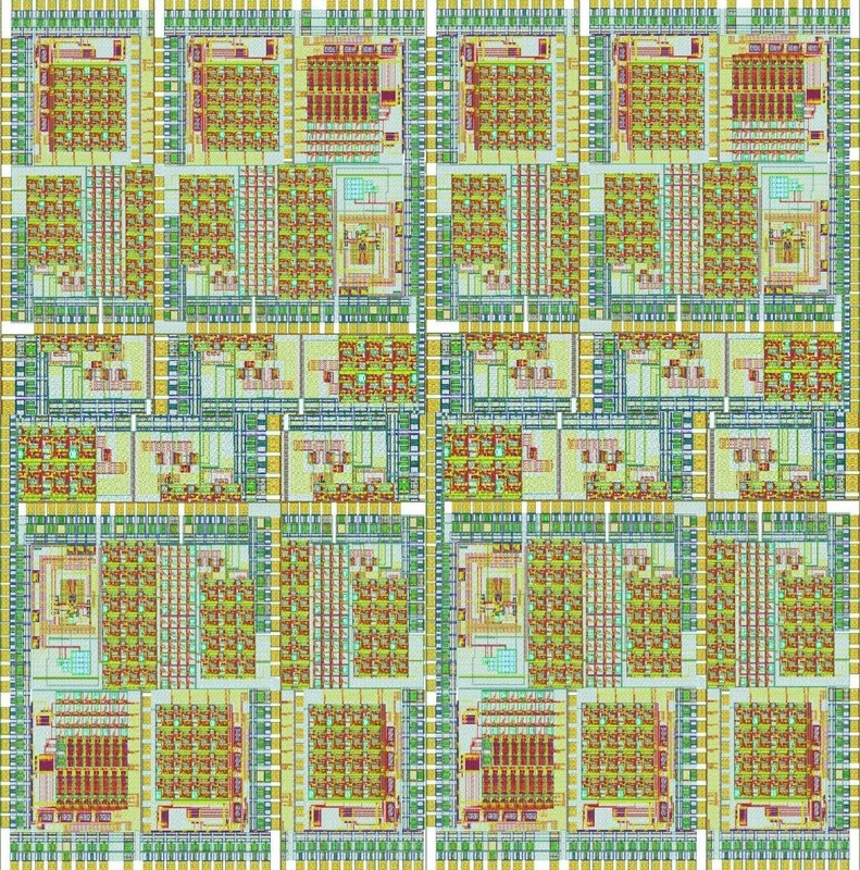
To understand why TSV technology could revolutionize computing, imagine the difference between a sprawling single-story warehouse and a towering skyscraper. Traditional chips spread their components—processors, memory, logic circuits—across flat silicon surfaces like a massive warehouse with long conveyor belts moving information between distant departments. TSV technology is like building skyscrapers for chips: instead of spreading components horizontally, you stack them vertically and connect them with ultra-fast elevators—the through-silicon vias [4][5].
Here’s why this matters for your smartphone, laptop, or any device with AI capabilities. Current chips waste enormous energy moving data across relatively long horizontal distances—imagine shouting across a football field instead of whispering to someone next to you. TSV technology shrinks these distances from millimeters to micrometers, potentially making AI processing 10-50 times more energy efficient [6][7].
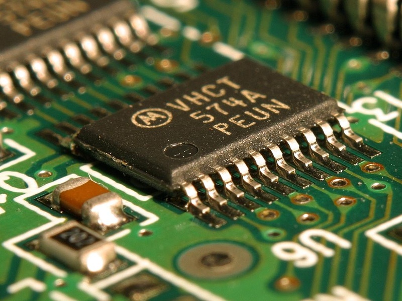
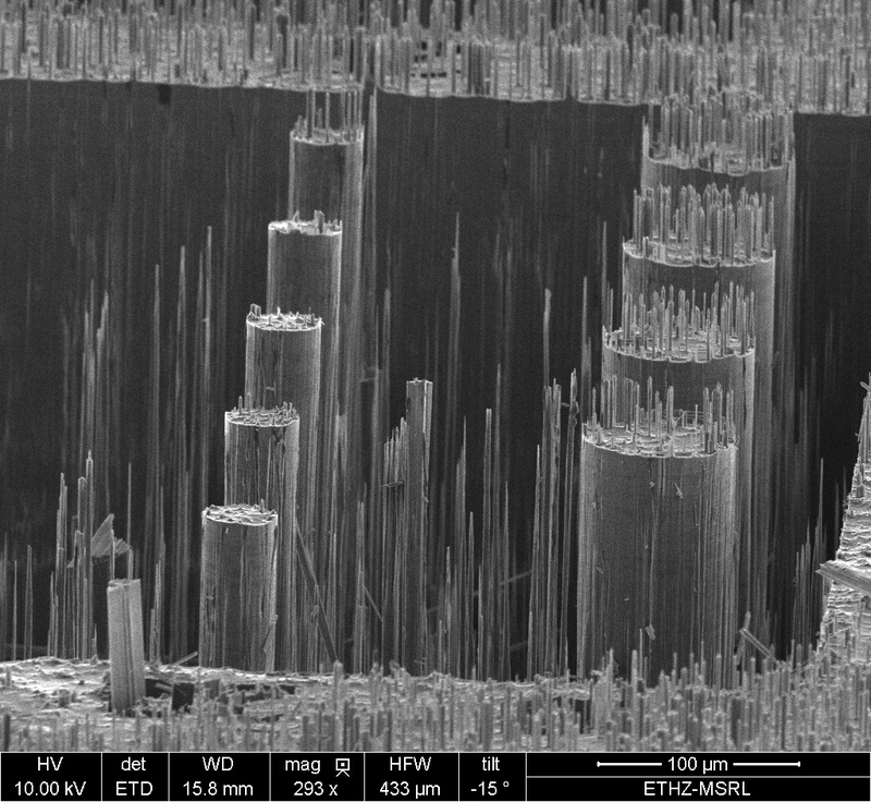
The engineering challenge is mind-bending. Engineers must drill holes 5-10 micrometers wide through silicon layers just 50 micrometers thick—imagine drilling a perfect tunnel through a sheet of paper using a drill bit the width of a virus. Then they fill each tunnel with copper so pure it conducts electricity flawlessly, even as the entire structure heats up and cools down thousands of times during normal use [8].
Advanced manufacturing techniques called deep reactive ion etching (DRIE)—essentially precision atomic sandblasting—can now create these tunnels with incredible accuracy. Think of it as using a controlled lightning bolt to carve pathways through silicon with the precision of a master sculptor working on the head of a pin. The newest processes can drill holes 10+ times deeper than they are wide while keeping the walls perfectly straight [9].
But here’s where engineering precision meets economic reality. TSV-based packaging costs 2-5 times more than traditional chip assembly, requiring companies to prove that the performance benefits justify the expense. For a smartphone manufacturer, this means asking: will consumers pay an extra $100 for AI features that work 10 times faster, or would they prefer the current speed at current prices? [1][10].
When Physics Meets Reality: The Heat Problem That Could Stop Everything
Imagine stacking 20 space heaters on top of each other, each one generating 200 watts of heat, then trying to keep them all from overheating in a space the size of a postage stamp. That’s essentially what happens when you stack multiple high-performance chips vertically using TSV technology. Each layer generates heat, but the layers in the middle have no direct path to cooling systems—they’re insulated by the very chips above and below them [9][12].
This heat problem isn’t just an inconvenience; it’s a potential showstopper. When chips get too hot—typically above 85°C (185°F)—they start making errors, slow down dramatically, or fail completely. It’s like trying to think clearly in a sauna while solving complex math problems: the hotter it gets, the worse your performance becomes.
Engineers have developed several clever solutions that sound like science fiction. Some designs include thermal superhighways—special TSVs dedicated entirely to conducting heat away from hot spots, like installing emergency cooling tubes throughout a burning building. Others integrate microscopic cooling channels directly into the silicon, allowing coolant to flow within micrometers of the hottest components [7][10].
Intel’s Foveros technology takes a different approach entirely: instead of stacking dozens of layers and fighting the heat, they optimize 2-4 layer configurations where thermal management remains practical. Think of it as building efficient mid-rise buildings instead of heat-trapping skyscrapers. This strategy sacrifices maximum density for reliable performance and cost control [10].
The thermal challenge creates a fascinating engineering trade-off. More sophisticated cooling solutions can handle higher heat loads, but they also increase manufacturing complexity, reduce reliability, and dramatically increase costs. Companies must decide: build simpler stacks that work reliably, or pursue maximum performance with expensive, complex thermal management that might fail in unexpected ways?
Economic Dynamics: Why TSV Success Depends on Market Forces, Not Just Physics
The most critical factor determining TSV technology’s commercial success isn’t thermal management or manufacturing precision alone—it’s the economic competition between semiconductor companies where massive R&D investments collide with equally large capital requirements for advanced packaging facilities. Understanding these dynamics reveals why technically impressive approaches sometimes lose to economically optimized solutions, and why the TSV market reflects broader industry consolidation trends.
TSMC’s strong position in advanced packaging stems from strategic integration of TSV development with their foundry services, allowing them to amortize development costs across a broad customer base. This business model enables sustained R&D investment in packaging technologies that smaller players find difficult to justify economically [1][8].
Intel’s major investments in advanced packaging capabilities, including TSV-based technologies like Foveros, represent a strategic decision to develop in-house capabilities rather than relying on external packaging providers. This vertical integration approach requires substantial upfront investment but potentially offers greater control over technology development timelines and cost structure [10].
The intellectual property landscape surrounding TSV technology adds complexity to competitive dynamics. Key patents are distributed among multiple companies, creating licensing requirements and cross-licensing agreements that can influence technology adoption decisions beyond pure technical merit [7].
Customer adoption patterns reveal additional economic considerations that extend beyond performance metrics. Companies like NVIDIA, AMD, and others must evaluate not just the technical benefits of TSV technology, but also the supply chain implications, design tool availability, and total cost of ownership when considering 3D integration approaches [2].
The semiconductor industry’s cyclical nature also influences TSV adoption. During periods of high demand and tight supply, customers may prioritize availability and proven technologies over cutting-edge approaches, while during periods of excess capacity, there may be more willingness to experiment with advanced technologies [1][8].
Market segmentation plays a crucial role in determining where TSV technology gains traction first. High-performance computing, AI accelerators, and aerospace applications may justify the additional cost and complexity, while cost-sensitive consumer applications may continue relying on traditional packaging approaches until costs decrease [12].
The Reality Check: From Laboratory Breakthroughs to Market Transformation
The transition from TSV technology’s promising laboratory demonstrations to commercial reality illustrates fundamental challenges in semiconductor innovation: technical capability doesn’t automatically guarantee market success. Early TSV prototypes demonstrated impressive achievements—dense via formation, multi-layer integration, and improved electrical performance compared to traditional interconnects. Yet these same technologies face significant challenges when transitioning from controlled laboratory conditions to high-volume manufacturing environments [5][7].
Manufacturing reliability has emerged as a key barrier to commercial TSV adoption. While laboratory TSV processes can achieve good electrical performance on test structures, production environments introduce contamination sources, equipment variations, and process stability challenges that can affect yield predictability. Maintaining consistent yields across different wafer lots and production timeframes requires sophisticated process control and monitoring systems [2][6].
The design ecosystem challenges proved equally significant in determining TSV adoption timelines. Designing chips for 3D TSV architectures requires new simulation tools, thermal modeling software, and design verification systems that had limited availability when the hardware technology was first developed. Major EDA companies have invested substantially in developing TSV-compatible design tools, representing development costs that are ultimately reflected in software licensing fees [7].
Customer adoption patterns revealed additional economic considerations: performance improvements don’t automatically justify higher costs and complexity. For many applications, the benefits achieved through TSV integration must be weighed against increased manufacturing costs and longer development timelines. Companies often find that optimizing existing 2D architectures can provide cost-effective performance improvements compared to transitioning to 3D TSV designs [1][8].
However, the economic equation changes for applications where TSV technology provides unique capabilities rather than incremental performance improvements. Applications requiring extensive interconnectivity between processing elements, such as certain AI accelerator architectures or specialized signal processing systems, may find that TSV technology enables computational approaches that aren’t practical with traditional packaging [10][11].
The most successful TSV commercialization strategies have focused on specific market segments where technical advantages align with economic realities. Rather than pursuing broad market adoption, companies have targeted high-value applications where TSV performance advantages justify premium pricing, providing revenue streams to support continued R&D investment while broader commercial adoption gradually develops [12].
References
[1] “3D Packaging vs 3D Integration eBook,” Semiconductor Engineering, accessed May 10, 2026.
[2] Lau, J.H., “Recent Advances and Trends in Multiple System Stacking,” IEEE Transactions on Components, Packaging and Manufacturing Technology, vol. 9, no. 12, pp. 2346-2358, 2019.
[3] Knickerbocker, J.U., et al., “3D Silicon Integration,” IBM Journal of Research and Development, vol. 52, no. 6, pp. 553-569, 2008.
[4] “Through-Silicon Via (TSV) Technology,” Applied Materials, company technical documentation, 2024.
[5] Banijamali, B., et al., “Advanced reliability study of TSV interposers and interconnects for the 28nm technology FPGA,” Electronic Components and Technology Conference, pp. 285-290, 2011.
[6] “ASE Group Homepage,” ASE Group, company overview, 2024.
[7] Garrou, P., et al., “Handbook of 3D Integration: Technology and Applications of 3D Integrated Circuits,” Wiley-VCH, 2019.
[8] “Advanced Packaging Solutions,” TSMC, technology documentation, 2024.
[9] Liu, X., et al., “Thermal management for 3D-IC with through silicon via,” International Symposium on Quality Electronic Design, pp. 1-6, 2011.
[10] “Intel Labs,” Intel Corporation, research overview, 2024.
[11] Yu, D., et al., “3-D Stacked CMOS Technology,” IEEE Transactions on Electron Devices, vol. 53, no. 11, pp. 2804-2812, 2006.
[12] “Samsung Foundry,” Samsung Foundry, technology documentation, 2024.
This digest was generated by AaBot using real-time web and literature research.