Semiconductor photolithography cleanroom with yellow safelight illumination and vacuum deposition equipment. Advanced packaging requires extreme precision to achieve the nanometer-scale tolerances needed for glass substrate processing. Credit: Wikimedia Commons

The Glass Revolution: How Intel's 10x Interconnect Breakthrough Is Rebuilding AI Chip Architecture from the Ground Up

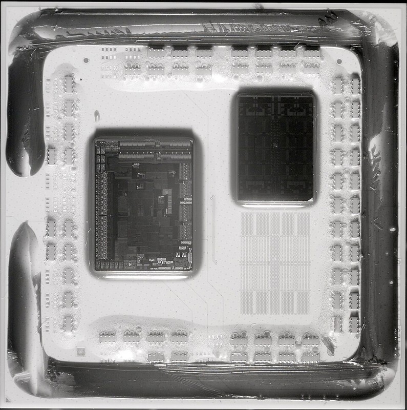
Glass substrates are replacing organic materials in advanced semiconductor packaging, enabling 10x higher interconnect density and solving the warpage crisis that threatens trillion-transistor AI processors. Intel’s glass core technology, launching in late-2027 data center products, delivers sub-2-micron via capabilities and thermal stability up to 200°C—making possible the massive multi-chiplet architectures needed for next-generation AI accelerators.

Shark skin denticles under electron microscope: millions of overlapping tooth-like structures channel water flow and reduce drag by up to 10%. These natural speed boosters inspire aircraft and ship hull designs. Credit: Wikimedia Commons

Nature's Speed Demons: How Sharks, Lotus Leaves, and Gecko Feet Are Revolutionizing Surface Engineering

Shark skin reduces drag by up to 12% through microscopic dermal denticles that control water flow, while lotus leaves achieve self-cleaning through hierarchical bumps that create superhydrophobicity. These natural superpowers now inspire artificial surfaces with enhanced drag reduction performance—opening applications from fuel-efficient aircraft to self-cleaning skyscrapers that never need washing.

Infrared thermal image of an AMD Ryzen processor showing the distinct chiplet architecture with separate dies for different functions. The color gradients reveal how chiplet design distributes heat more efficiently than monolithic chips. Credit: Wikimedia Commons

The 1000-Core Revolution: How Chiplet Integration and 3D Stacking Are Redefining the Limits of Computing Power

Modern processors now integrate over 1000 specialized cores through chiplet architectures that combine multiple silicon dies into unified systems, while 3D stacking technologies enable 8.4 TFLOPS performance at just 4.3W power consumption. This heterogeneous approach allows mixing cutting-edge 3nm logic with mature 14nm memory on a single package, delivering 10x better power efficiency than traditional monolithic designs while reducing costs by 40%.

NASA's Perseverance rover captured by the Sky Crane descent stage camera moments before touchdown in Jezero Crater, February 2021 — the first image of a Mars landing in progress. Credit: NASA/JPL-Caltech

Beyond Radio Silence: How AI Pilots Spacecraft Through the Solar System's Deep Unknown

ESA’s Hera mission demonstrates AI-driven autonomous navigation that makes real-time decisions during its 2-year journey to asteroid Didymos, while NASA’s Enhanced AutoNav enables Mars rovers to traverse 320 meters daily without Earth commands. This represents a fundamental shift from ground-controlled missions to truly independent spacecraft that navigate, explore, and adapt using onboard artificial intelligence.

A semiconductor wafer diffracting light into a vivid rainbow spectrum — the nanoscale periodic structures etched into wafers like these are what make 2D materials so promising for next-generation electronics. Credit: Wikimedia Commons

Beyond Graphene: Transition Metal Dichalcogenides Reshape AI Hardware and Quantum Computing

While graphene captured early 2D materials attention, transition metal dichalcogenides like MoS2 now power breakthrough applications from neuromorphic AI chips to room-temperature quantum processors. Unlike graphene’s zero bandgap limitation, TMDs offer tunable semiconducting properties spanning 1-3 eV, enabling direct integration into digital logic and quantum devices without the complex bandgap engineering that hobbled graphene commercialization.

Infrared thermal imaging of electronic components reveals hotspots reaching 84°C — the kind of thermal challenges that metamaterial-based phononic crystals aim to solve. Photo: Wikimedia Commons

Metamaterials and Phononic Crystals: Engineering Heat Flow at the Nanoscale for Next-Generation Thermal Management

MEMS bolometer experiments demonstrate 2-3x enhanced thermal sensitivity through phononic crystal integration, while advanced metamaterial designs achieve thermal conductivity control spanning five orders of magnitude. AI-accelerated optimization reduces design cycles from weeks to hours for next-generation thermal management.

RISC-V architecture diagram showcasing the open-source approach to processor design

RISC-V Open Source Processor Ecosystem: Transforming Semiconductor Innovation Through Open Standards

RISC-V’s open instruction set architecture is revolutionizing processor design with over 4,500 RISC-V International members and commercial deployments including Espressif’s ESP32-C3 microcontrollers, enabling customizable processors without licensing fees while fostering unprecedented collaboration between academia and industry.